Light-shrinking' layer converts regular microscope to super resolution imager
UC San Diego's method coats microscope slide with metamaterial composed of fine layers of silver and silica.
01 June 2021 Research & Development
 Electrical engineers at the University of California San Diego have developed a technology that improves the resolution of an ordinary light microscope so that it can be used to directly observe finer structures and details in living cells.
The group's technology turns a conventional light microscope into a super-resolution microscope. It involves a specially engineered material that shortens the wavelength of light as it illuminates the sample; this shorter wavelength light is what enables the microscope to image in higher resolution.
"This material converts low resolution light to high resolution light," commented Zhaowei Liu, a professor of electrical and computer engineering at UC San Diego. "It's very simple and easy to use. Just place a sample on the material, then put the whole thing under a normal microscope-no fancy modification is needed."
 The work, which was published in Nature Communications, overcomes a significant limitation of conventional light microscopes: their low resolution. Conventional optical microscopes are useful for imaging live cells, but they cannot image anything smaller.
'Hyperbolic metamaterial'
Conventional light microscopes typically have a resolution limit of 200nm, meaning that any objects closer than this distance will not be observed as separate objects.
While there are more powerful tools available, such as electron microscopes, which have the resolution to see subcellular structures, they cannot image living cells because samples need to be placed inside a vacuum chamber.
"The major challenge is finding one technology that has very high resolution and is also safe for live cells," added Liu. The technology that Liu's team developed combines both features. With it, a conventional light microscope can be used to image live subcellular structures with a resolution of up to 40nm.
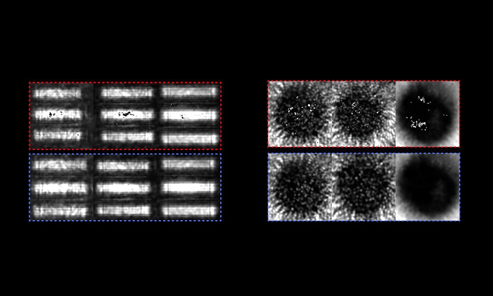
 and coated with metamaterial (r).") The technology consists of a microscope slide that's coated with a type of light-shrinking material called a hyperbolic metamaterial. It is made up of nanometers-thin alternating layers of silver and silica glass. As light passes through, its wavelengths shorten and scatter to generate a series of random high-resolution speckled patterns.
The technology consists of a microscope slide that's coated with a type of light-shrinking material called a hyperbolic metamaterial. It is made up of nanometers-thin alternating layers of silver and silica glass. As light passes through, its wavelengths shorten and scatter to generate a series of random high-resolution speckled patterns.
When a sample is mounted on the slide, it gets illuminated in different ways by this series of speckled light patterns. This creates a series of low resolution images, which are all captured and then pieced together by a reconstruction algorithm to produce a high resolution image.
The researchers tested their technology with a commercial inverted microscope. They were able to image fine features, such as actin filaments, in fluorescently labeled Cos-7 cells-features that are not clearly discernible using just the microscope itself. The technology also enabled the researchers to clearly distinguish tiny fluorescent beads and quantum dots that were spaced 40 to 80 nanometers apart.
'Great potential for high-speed operation'
The super resolution technology has great potential for high speed operation, the researchers said. Their goal is to incorporate high speed, super resolution and low phototoxicity in one system for live cell imaging.
Liu's team is now expanding the technology to do high resolution imaging in three-dimensional space. This current paper shows that the technology can produce high resolution images in a two-dimensional plane. The team previously published a paper showing that this technology is also capable of imaging with ultra-high axial resolution (about 2nm). They are now working on combining the two together.
This work was supported by the Gordon and Betty Moore Foundation and the National Institutes of Health (R35 CA197622). This work was performed in part at the San Diego Nanotechnology Infrastructure at UC San Diego, a member of the National Nanotechnology Coordinated Infrastructure, which is supported by the US National Science Foundation.

Trumpf hopeful of a recovery as orders tick up
July 28 2026

Computational optics startup Elio raises $21M
July 28 2026