
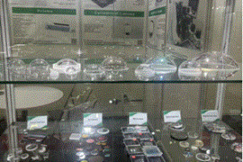
Another selection of significant announcements from the optical communications expo in Los Angeles.
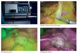
Collaboration with Sony designed to enhance visualization during minimally invasive surgeries.
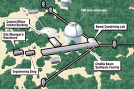
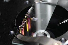
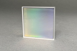
Delay line control system intended to improve precision and interferometric capabilities.

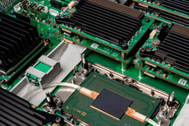
...while imec and New Origin partnering to scale SiN photonic IC manufacturing.
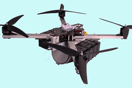
In UAV strike and reconnaissance operations, optical communication systems are delivering a decisive advantage.
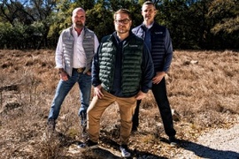
Albuquerque startup emerges from stealth mode with approach to power satellites while they are in Earth's shadow.
 17 Mar 26 |
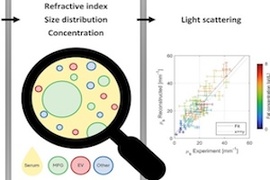
University of Twente reveals optical properties of human milk Light-scattering data give insights into milk composition. |
 17 Mar 26 |
Fiber laser startup Femtum raises $16M Canadian startup looking to target trimming applications in silicon photonics with mid-infrared sources. |
 17 Mar 26 |
Fiber networks now pass 295 million homes across Europe FTTH Council Europe releases report on continental progress ahead of London conference in April. |
 17 Mar 26 |
Chalmers miniaturizes biosensor for smaller and cost-effective devices Metasurface-based approach offers scalability for diverse applications and mass manufacture. |
 16 Mar 26 |
CU Boulder develops novel vacuum UV laser Offers potential to improve nanotechnology and power nuclear clocks. |
 12 Mar 26 |
OFC 2026 to showcase high-speed optical networking and interoperability “Sold-out exhibition, as AI-driven network demand fuels surge of major product debuts and breakthroughs.” |
Master Bond Inc.
ECOPTIK
Voltage Multipliers, Inc
Resolve Optics Ltd
Hamamatsu Photonics Europe GmbH
Wasatch Photonics
 | Impact of Backgrounds on Virtual Image Quality in AR Glasses 24 Feb Instrument Systems Discover our whitepaper, “Impact of Backgrounds on Virtual Image Quality in AR Glasses.” Optical see-through AR promises seamless overlays, yet real-world backgrounds reshape contrast, color, and uniformity of the virtual image. We quantify how luminance, chromaticity, and spatial structure constrain influence the virtual image using calibrated photometric and colorimetric measurements and additive color-mixing analysis. Learn key trade-offs between visibility and transparency – and optimization guidance for AR systems. |
 | Imaging solutions: Driving agri-food tech towards sustainability 01 Mar Hamamatsu Photonics Europe Photonics and imaging technology have become crucial for sustainable farming, aiding crop health monitoring, resource optimization, and waste reduction. Hamamatsu Photonics’ InGaAs sensors and cameras, sensitive in the VIS, NIR, and SWIR regions, support void detection and damage inspection, enhancing yields, reducing environmental impact, and ensuring food safety and quality. |
 | Choosing the best spectrometer for NIR OCT 02 Apr 2025 Wasatch Photonics Near infrared optical coherence tomography has traditionally been limited to imaging depths of just a few millimeters, but with our expanded line of OCT spectrometers, up to 12 mm is possible. In this tech note, we explore and compare three different drop-in spectrometer models designed to serve a wide range of resolution, depth, and size requirements in NIR OCT imaging. |
 | Identifying Optical Materials with Precision Accuracy 04 Mar 2025 Knight Optical Precision accuracy is a critical necessity with any optical component. Rigorous testing to ensure strict compliance with given requirements will always be essential; it is a vitally important demand within any industry sector. Dimensional, surface profiling and optical performance testing are significant aspects of this process, but an additional layer of assurance and quality can be achieved with the use of material verification, employing methods such as refractive index, density testing and transmission measurement. This White Paper explores advanced techniques for precise optical material verification, overcoming the limitations of traditional testing methods. |


 |
 |
 |
 |
 |
| © 2026 SPIE Europe |
|


