imec-led consortium to develop chip roadmap ‘beyond CMOS’
While imec and New Origin partnering to scale SiN photonic IC manufacturing.
18 March 2026

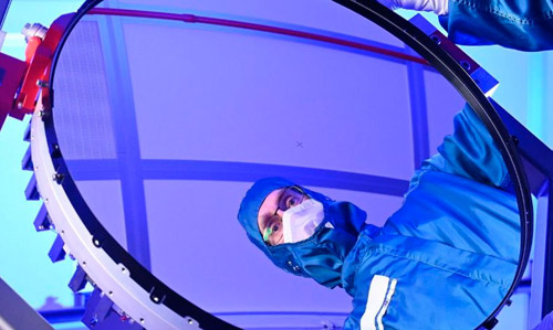
| Alongside 26 universities, group will use NanoIC pilot line to improve function and design of “CMOS 2.0” chips. Image: imec. |
imec, a Belgium-based research and innovation hub for nano- and semiconductor technologies, has launched a consortium with 26 European university groups to work on the technology roadmap looking beyond CMOS scaling, so-called “CMOS 2.0”.
The initiative is to focus on design automation and architecture research for future chips. The consortium will benefit from the NanoIC pilot line, to advance academic insights into industry-focused innovations. In the future, states imec, similar consortia will be set up around advanced materials and alternative compute systems.
CMOS 2.0 refers to a new paradigm, introduced by imec, that expands the chipmaking toolbox beyond traditional transistor scaling and its associated scaling challenges. CMOS 2.0 allows for more design flexibility by exploiting fine-grain wafer stacking technology to improve on-chip connectivity and offer higher technology heterogeneity to the system.
Funding 26 PhDs
The new research program will require cooperation between different areas of the chip ecosystem. Within imec’s CMOS 2.0-consortium, 26 PhDs will be funded. The PhD students will stay at their home university, embedded in their research group, allowing them to tap into complementary fields of expertise and stimulate cross-fertilization, says the announcement.
Sahar Sahhaf, Director of Academic Partnership Development at imec, commented: “Leveraging the benefits in both connectivity and heterogeneous integration enabled by 3D wafer stacking will reshape every stage of design and chip architecture. It is the first time that imec is bringing together such a network of premium European university teams in a structured way to have guided contributions to the future semiconductor roadmap.”
Mehdi Tahoori, Technical Director, at imec added, “This university research consortium aims to infuse CMOS 2.0 technology to the entire design stack, from Electronic Design Automation all the way to system architecture. It aims to stimulate the broader research and academic community on various aspects of the CMOS 2.0 revolution.”
Partnership members
The CMOS 2.0 university consortium consists of following universities:
- National Technical University of Athens
- Delft University of Technology
- École Polytechnique Fédérale de Lausanne (EPFL)
- Eidgenössische Technische Hochschule Zürich
- Karlsruhe Institute of Technology
- Katholieke Universiteit Leuven
- KTH Royal Institute of Technology
- LIRMM, University of Montpellier, CNRS
- Politecnico di Torino
- Sabancı University
- Universidad Complutense de Madrid
- Universiteit Gent
- Université libre de Bruxelles
- University of Thessaly

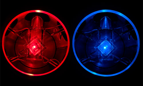
imec and New Origin to scale Photonic IC manufacturing
In related news, New Origin, a photonic chiptech foundry, is to work with imec, to address the need to scale silicon nitride-based photonic IC (PIC) manufacturing in an industrial environment. This collaboration is also intended to strengthen the European photonics supply chain and enable New Origin to scale up imec’s LPCVD silicon nitride technology platform to meet customer demand.
In the proposed arrangement, imec will transfer its proven LPCVD silicon nitride PIC platform to New Origin to support growing demand for photonic chips for consumer, health, datacom, defense, and quantum applications. imec will help to scale the manufacturing on 200mm wafers using photolithography in New Origin’s industrial facilities, which also support non-CMOS-compatible processes and materials.
Twan Korthorst, CEO of New Origin, said, “This collaboration allows us to shorten the time to volume production for customers, and it strengthens the industrialization of PIC technology in Europe. With our plans to develop towards a manufacturing capacity of 50,000 wafers per year, New Origin will strengthen the European supply chain of PICs and unlock the next wave of innovation.”
Philippe Absil, of Silicon Solutions at imec, said, “imec has demonstrated that silicon nitride photonics can unlock exceptional performance and scalability. Our SiN platform can deliver ultra low loss in a wide wavelength spectrum ranging from visible to short wave infrared making it ideal for applications in bio-sensing, AR/VR and datacom, as well as quantum applications on the horizon.”


Fraunhofer IOSB model reliably detects deepfakes
July 16 2026