 |
Date Announced: 20 Jan 2026
Advancing Thermal Scanning Probe Lithography
Zurich, Switzerland — Following the successful introduction of the modular NanoFrazor nanolithography system in 2024, Heidelberg Instruments is proud to announce the installation of the newest NanoFrazor. The system is equipped with the recent modules, enabling parallelized thermal scanning probe lithography (t-SPL). The beta site is hosted by the research partner EPFL, the Swiss Federal Institute of Technology in Lausanne, Switzerland. The installation marks a significant step forward in joint efforts to bring next-generation nanofabrication technologies into practice, promising advances in nanoscale research and applications.
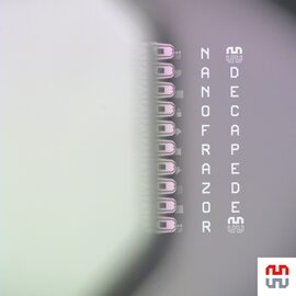
Designed for high-resolution lithography down to 20 nm, with application flexibility and increased throughput, the system features parallelized t-SPL with ten heated tips writing simultaneously, Direct Laser Sublimation (DLS), and advanced automation. “Parallelizing t-SPL was the logical next step in advancing thermal nanolithography. The implementation, however, was far from trivial.” states Dr. Emine Cagin, CTO of Heidelberg Instruments Nano AG. “Parallelization required a decade of development, culminating in a new and scalable framework for electronics and software that now powers the new NanoFrazor.”
The new module, named the Decapede, increases the throughput up to tenfold, without compromising on high-resolution capabilities. “With improved throughput, we are considering upscaling grayscale nano surfaces that enable deterministic and localized strain engineering of 2D materials from chip-level to wafer-scale for potential industrial integration”, says Berke Erbas, Postdoctoral Researcher in the Microsystems Laboratory at EPFL. “We also aim to upscale grayscale nanoimprint lithography stamps fabricated through t-SPL and dry-etching approaches.”
EPFL — A Hub for Innovation
EPFL’s expertise in t-SPL and broad nanofabrication capabilities make it an ideal beta site and mark the continuation of a long-standing, trusted partnership with Heidelberg Instruments. The consortium of research groups involved brings together a combination of deep knowledge in t-SPL and diverse nanofabrication techniques, along with fresh ideas and challenging applications. The generous commitment to providing continuous feedback will help Heidelberg Instruments further validate the system performance and refine user interfaces.
From Nanoelectronics to Quantum Devices, a Look Ahead
The EPFL beta site is not only a testing and validation site for the system’s capabilities but first and foremost a catalyst for innovation in nanolithography. Applications at the EPFL beta site span nanoelectronics, plasmonics, quantum devices, and bio-nano-sensors. Jürgen Brugger, Professor in Microengineering and Materials Science at EPFL, highlights: “t-SPL has proven to be an excellent tool for educating junior researchers due to its capabilities for fast prototyping with a low threshold to create nano-patterns in short time scales. We are excited to expand towards parallel writing capabilities.” For example, the Laboratory of Nanoscience for Energy Technologies (LNET), Professor Giulia Tagliabue, is exploring the use of its gray-scale functionalities for realizing advanced metasurfaces that can strongly confine light at nanoscale dimensions for energy conversion and probing of interfacial processes.
We are looking forward to seeing how the beta site will accelerate discoveries and enable new possibilities in nanoscale science, both in research and educational use of the NanoFrazor system.
Further information: https://heidelberg-instruments.com/product/nanofrazor/
https://heidelberg-instruments.com/
About Heidelberg Instruments
With over 40 years of experience and more than 1,500 systems installed across 50+ countries, Heidelberg Instruments is a global leader in the design, development, and production of high-precision laser lithography systems, maskless aligners, and nanofabrication tools. The product portfolio ranges from compact tabletop solutions to high-end photomask manufacturing equipment. This flexibility makes the systems indispensable to leading universities, R&D institutes, and industrial facilities worldwide. The versatile systems enable precise surface structuring on the micro- and nanoscale, supporting both 2D patterning and 2.5D features through grayscale lithography for applications in photonics and micro-optics, electronics, semiconductors, quantum technology, MEMS, microfluidics, 2D materials, and beyond.
| © 2026 SPIE Europe |
|