imec collaboration integrates InP lasers with silicon photonics
Precision alignment with large-scale wafers to be offered as a prototyping service later this year.
08 June 2021 Research & Development

A European collaboration between silicon photonics researchers and a semiconductor equipment firm says it has successfully integrated indium phosphide (InP) lasers with silicon photonics on an industrial-scale wafer platform.
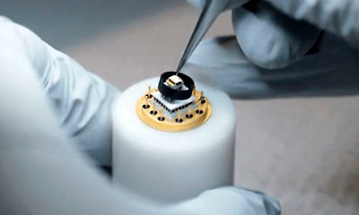
The work, led by Belgian electronics institute imec alongside Sivers Photonics (formerly CST Global) and equipment firm ASM AMICRA Microtechnologies, uses a flip-chip bonding tool for high-precision alignment.
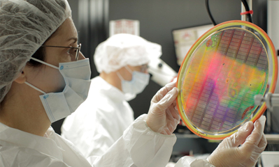
imec reports that the team was able to bond InP distributed feedback (DFB) laser diodes onto a 300 mm diameter silicon photonics wafer with an alignment precision within 500 nanometers.
That enabled reproducible coupling of more than 10 mW of laser power into the silicon nitride waveguides on the silicon photonics wafer - something that is typically hampered by high coupling losses.
Prototyping service
imec says that it plans to offer the new technology platform as a prototyping service later this year, with the aim of accelerating the adoption of silicon photonics in cost-sensitive applications like optical interconnects, lidar, and biomedical sensing.
Following initial work with CST Global completed in March 2020, imec had originally planned to begin offering the service in the first half of this year.
After it does become available, the hybrid integration portfolio will be extended with reflective semiconductor optical amplifiers (RSOA), exploiting the etched-facet capability of Sivers' "InP100" technology, and ASM AMICRA's "NANO" flip-chip bonder tool.
"This capability will enable advanced, external cavity laser source types, as required for emerging optical interconnect and sensing applications, and will become available in early 2022," imec said.
Prototype PICs
Joris van Campenhout, the director of imec's Optical I/O Program, said: "This additional functionality will enable our joint customers to develop and prototype advanced photonic integrated circuits (PICs) with capabilities well beyond what we can offer today, in key areas such as datacom, telecom, and sensing."
Sivers Photonics managing director Billy McLaughlin added: "The availability of InP laser sources, designed and fabricated on our InP100 manufacturing platform, will boost the adoption of silicon photonic circuits for a wide variety of commercial applications."
Johann Weinhändler, the managing director at ASM AMICRA, observed: "Our strength in high-precision placement seamlessly complements the expertise of all partners.
"With automated and ultra-precise flip-chip bonding, the way to high-volume manufacturing of these hybrid assemblies is open."
Laser-etched synthetic skin resists icing at -50 °C
March 30 2026


