Dental laser system vendor initiated Chapter 11 proceedings earlier this month; the two firms were engaged in patent litigation.
Singapore startup says that its scalable silicon-based devices also offer low power consumption.
Novel method for surface flaw detection on glossy and flat materials impressed the jury, out of more than 60 entries.
Freeform dual comb spectroscopy creates images of methane plumes not visible to the human eye.
Association’s MV department expects national decline in sales for image processing sector in 2024.
Design based on integrated silicon photonics expands utility of optical tweezers for biological research.
Fraunhofer IAF achieves first operation of dual-media NV diamond laser “Laser threshold magnetometry” offers many medical diagnostics and treatment processes. |
Nuburu agrees $65M equity-plus-credit deal Developer of blue industrial lasers to receive weekly capital infusion and access to $50M credit line. |
Megahertz OCT improves view of tumor margins and brain anatomy
University of Lübeck integrates faster OCT into commercial neurosurgical microscope. |
SPIE Photonics Summit highlights business opportunities with US Government Third annual meet-up in Washington DC brings together big hitters from industry and policy-makers. |
Zeiss names new CEO after Lamprecht decides not to extend contract Semicon manufacturing chief Andreas Pecher steps up to lead role, from April 2025. |
Arizona opens new home for the Center for Quantum Engineering
Wyant College of Optical Sciences has moved the CQN into the new “quantum floor”. |
ECOPTIK
Resolve Optics Ltd
Hamamatsu Photonics Europe GmbH
Making Raman Measurements Reproducible 28 Mar Wasatch Photonics Raman OEM applications need consistent spectra to deliver dependable answers. A good-quality OEM spectrometer should, by design, exhibit low unit-to-unit variability from the start, and any remaining small differences should be corrected in order to achieve the most robust and repeatable analytical outcomes in the field. Learn how to achieve >99.5% unit-to-unit agreement using a series of simple corrections. |
Improving Calibration Accuracy for High-End Spectroradiometers 06 Oct 2023 ADMESY BV Admesy introduces a groundbreaking calibration concept that surpasses the limitations of conventional calibration light sources. |
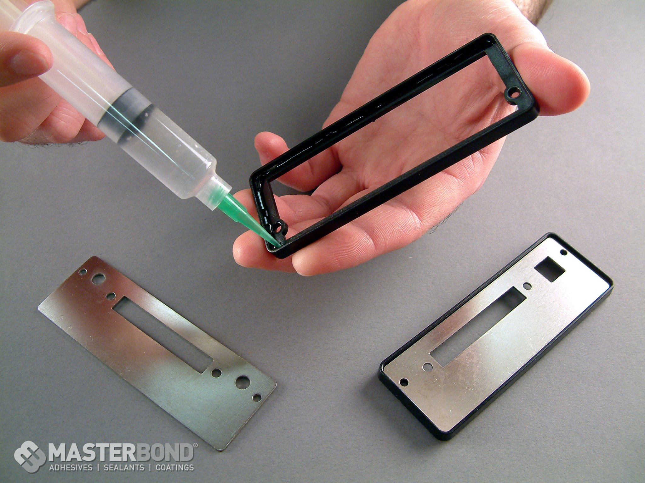
UV Curing Adhesive Used in Electro-Optical Studies 07 Jun Master Bond Electro-optical (EO) polymers offer several advantages over inorganic materials in the fabrication of optical waveguide structures. Master Bond UV15 has been selected for use in the fabrication of polymer optical waveguides for a variety of applications. Read this case study to learn more about how UV15 helped the researchers achieve their goal. |
Microscopy Objective Lens Metrology 13 Sep Optikos Today’s microscopy systems push the limits of performance and engineering. The advent of digital microscopy and computational processing means, whether using a manual laboratory microscope or a high-throughput automated platform, instruments are expected to produce excellent image quality across a large FOV and across a range of wavebands. To understand the performance limits of cutting-edge optical systems you need high-quality, reliable, and precise metrology systems. |
© 2024 SPIE Europe |
|