|

20 May 2010
Growing gallium arsenide in thick multilayer stacks could make a big difference to the cost of compound semiconductor devices.
The fabrication of photovoltaics and optoelectronic devices such as near-infrared (NIR) imagers looks set to become significantly easier thanks to a new way of growing layers of compound semiconductor material. Having perfected the technique for gallium arsenide (GaAs), the team hopes that its method will be equally applicable to other material systems such as gallium nitride and indium phosphide (Nature 465 329).
"We can generate compound semiconductor devices much more cheaply than previously possible," John Rogers from the University of Illinois at Urbana-Champaign, US, told optics.org. "We can also integrate these devices with a much wider range of substrates, including glass and plastic. In photovoltaics, we expect the cost reductions to be significant, and that the ability to put cells on thin sheets of flexible plastic will increase the mechanical robustness and the modes for use."
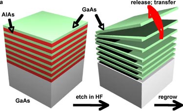
When it comes to growing compound semiconductors such as GaAs, the conventional approach involves epitaxial growth of a thin layer of active material onto the surface of a bulk wafer, which in turn is diced into smaller pieces. This method is costly for two reasons. First, it consumes the underlying wafer even though it plays no role in the final device and second, the active material can only be grown in thin layers at a time.
The technique being pioneered by Rogers and colleagues involves growing GaAs in thick, multilayer stacks and then separating these layers from one another (and from the underlying wafer) and printing them on to a substrate.
This strategy does not consume the wafer, which can be reused for many rounds of growth, and allows GaAs to be grown in thick, bulk quantities in each growth run. The size of the GaAs layers can range from micrometers to centimetres and thicknesses from several nanometers to microns.
According to Rogers, the two main challenges were developing growth methods that offer the same high materials quality that is possible in thin, single layer configurations and finding a way to release the layers from one another and print them onto other substrates.
"We use an elastomeric pad to gently lift individual layers," explained Rogers. "This pad can then print these pieces onto a substrate of interest. The pad is very soft and rubbery to avoid fracturing the layers during this process."
To demonstrate the versatility of this technique, the team has already grown multilayer stacks for metal semiconductor field effect transistors (MESFETs), Schottky diodes, NIR photodetectors and single-junction photovoltaics. These devices were formed on glass, silicon and PET substrates respectively and, according to Rogers, their performance was on par with devices fabricated by traditional methods.
The team is now working with other materials, such as gallium nitride for LEDs. "In parallel, we are working closely with a company called Semprius, which is commercializing this technology for applications in photovoltaics," said Rogers.
 |  |  |  |  |  |  |
| © 2026 SPIE Europe |
|