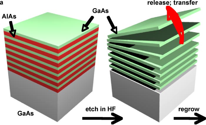
| MOCVD forms multiple layers of GaAs with separating layers of AlAs. Patterned vertical etching exposes the sidewalls. Immersion in hydrofluoric acid selectively eliminates the AlAs layers, thereby releasing the layers of GaAs. The size of the GaAs layers can range from microns to centimetres and thicknesses from several nanometers to microns. (Courtesy: John Rogers) |
| © 2026 SPIE Europe |
|