|

02 Mar 2010
Two-element VGA lens points the way to higher-resolution wafer-level cameras for ultraslim mobile phones
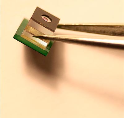
Nemotek Technologie (Rabat, Morocco) is hoping to win big with a new lens made from two optical wafers that are processed separately and then bonded together before being diced.
Unveiled last month at the Mobile World Congress in Barcelona, the two-element lens also incorporates an infrared filter and apertures into the lens structure so as to reduce the number of components within a wafer-level-camera (WLC) module. Nemotek believes that this integrated functionality will allow WLCs to be incorporated into new ultraslim mobile phones and notebook computers.
"This is the starting point, opening the door to higher megapixel resolutions in wafer-level cameras," said Hatim Limati of Nemotek. "Lenses with at least two elements will be required as camera resolutions rise. Now that we have shown how to align two glass wafers together and dice them to produce high-quality lenses, the way towards 2 or 3 megapixel resolution is open."
A two-element lens produces improved sharpness and higher image quality compared to a one-element structure. What is more, the new components can be incorporated into standard reflow manufacturing processes with a minimum of adjustment.
"Controlling the 'reflowability' was one of the three critical goals during the development of the new lens, the other two being the size and the cost," said Limati. "Our aim was to show that with the new lens we could increase the megapixel resolution but still keep the camera small."
Despite the successful demonstration of a two-element lens, Limati commented that Nemotek's roadmap does not involve adding lens elements in increasing numbers.
"With conventional lenses, the more you increase the pixel resolution, the more elements you have to add to the lens. But we are not announcing a two-element lens today as a step to a three- or four-element lens in the future. The real advantage of wafer-level technology is the control it gives you over the size of the of the camera, and that's the factor that will have an impact in the market niches that these components will serve."
Those niches also include webcam units in computers, where the improved image quality from a two-element lens could become a selling point. Lower-price computers normally use VGA optics, but some high-end brands wish to move towards webcams capable of 1.3 megapixel resolution, which requires better-quality optics than is possible with a one-element lens. The Nemotek component could allow that improvement without a substantial cost penalty.
"Computer manufacturers are continually refining the style of their products and improving the quality of their screens, and they want to match that with a corresponding improvement in the quality of the camera," commented Limati. "But they don't want to increase the overall size of the sensor. Not only would that make the device more expensive, but design constraints arising from the size of the laptop or the design of the lid can be an issue. A two-element VGA wafer-level lens is a very competitive technology for solving that problem while remaining within manufacturers' design limits. It's all about matching application needs."
 |  |  |  |  |  |  |
| © 2026 SPIE Europe |
|