
Metasurface-based approach offers scalability for diverse applications and mass manufacture.
Offers potential to improve nanotechnology and power nuclear clocks.
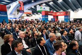
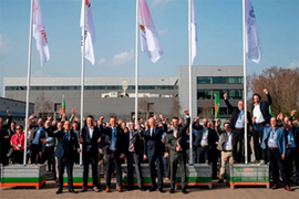
“Sold-out exhibition, as AI-driven network demand fuels surge of major product debuts and breakthroughs.”
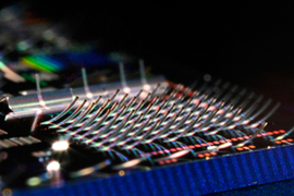
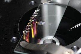
Photonic device that curls beam off chip surface could advance displays, communications, quantum computing.
UMC and Wavetek sign a strategic manufacturing partnership in bid to commercialize TFLN photonics.

Santa Clara startup also launches eight-wavelength laser based on its proprietary frequency-comb approach.

Chip giant plans to more than quadruple capacity for 'PIC 100' process by next year.
Novel photonic chips promise better AI data centers, 6G networks, super computers.
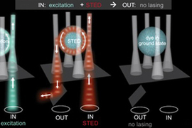
Researchers demonstrate nanosecond optical switching using a dye-doped droplet that redirects stored energy without electrical input.
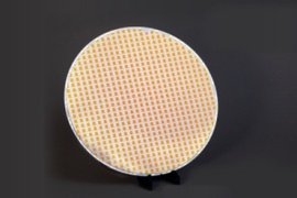
Raman has significant potential for assessing stability of mRNA vaccines.
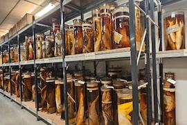
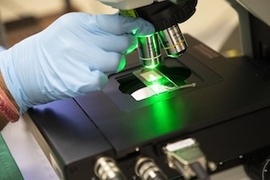
Agilent and STFC use spatially offset Raman technique in museum setting for the first time.
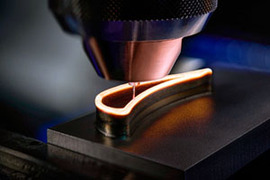
Cailabs is contributing new compact process head based on its MPLC beam shaping technology.
| © 2026 SPIE Europe |
|


