 |

14 Dec 2007
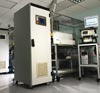
Developing lasers that process plasma display panels at rates of up to six metres per second is commonplace at UK firm Powerlase. Mike Mason and Matt Henry tell Jacqueline Hewett about the company's technology and the new opportunities that are on the horizon.
When a company that has been in existence for just six years reports that its 2006 turnover grew 400% year on year, it must be doing something right. That's the current situation at UK firm Powerlase who, thanks to a realistic long-term business plan and a clever optical technology, quotes that its lasers are now used in 60% of today's global plasma display panel (PDP) manufacturing.
Powerlase's success is rooted in the fact that it produces "the world's most powerful nanosecond Q-switched diode-pumped solid-state (DPSS) lasers". Flat-panel display giants such as LG Electronics and Samsung SDI are adopting this technology thanks to the combination of substantial cost savings and increased production capacity.
"We are specifically looking to displace wet-etch lithography for patterning thin films and our biggest single advantage is cost of ownership," Matt Henry, Powerlase's head of applications engineering, told OLE. "We have had most impact to date in PDP manufacture. We have compelling models that are endorsed by our customers, who can potentially save more than $150 m in running costs per production line with identical output over a three-year period."
The business plan
Turn back the clock six years to 2001 and it was an entirely different story. Powerlase was a fledgling firm newly spun out of London's Imperial College anxious to attract venture-capital funding to get its ideas off the ground. "Initially we were producing extreme ultraviolet (EUV) sources for semiconductor lithography, but it was always a long-distance market," Mike Mason, the company's vice-president of technology, explained. "We also identified that our lasers could be used for flat-panel display manufacture and that was an emerging market at the time. In order to make money in the short term, we concentrated on this application. EUV is still there and will hopefully come to fruition in the next few years."

Today, after attracting substantial venture capital funding as well as volume orders for its products, Powerlase is operating out of a 20,000 ft2 facility, has a sales and service centre in Korea, and a workforce of around 50. "We have been careful not to explode too fast," said Mason. "When I started in 2001, I was the 10th employee, so it has been organic growth."
So what does Powerlase see as the secret to its success? "The key thing, and this is less common than you might think, is that we are entirely customer driven," explained Mason. "We talk to our customers on a regular basis – particularly our Asian customers who value face-to-face contact very highly. We try to give the customer exactly what they want."

Being a relatively small company compared with its competitors, Powerlase also rates its flexibility as a key advantage. "Our customers guide us and we can provide them with what they want, when they want it and how they want it," added Henry. "It is easy to sell a clever piece of technology once, but to sell it in volume and to get repeat orders requires people to have confidence and believe in you. That is what we have achieved."
Scalable technology
Powerlase's expertise lies in developing Q-switched DPSS lasers that produce nanosecond pulses with high average powers and high peak powers. At the heart of the laser is a gain module, the precise design of which is a carefully guarded secret.

"We use diode lasers to side pump a YAG rod inside the gain module," explained Mason. "The key to our performance is in the detailed design. This module provides a scalable architecture that gives us the capability to produce a range of powers and frequency convert to different wavelengths. We have IP covering the cavity formed around the module and the way that we cope with the high powers produced via acousto-optic Q-switching, which is non-trivial."
The end result is a DPSS laser system that produces pulses with a duration of tens of nanoseconds at repetition rates of tens of kilohertz at 1064, 532 and 355 nm. The company says that its infrared lasers can produce average powers ranging from 200 to 1600 W, peak powers in excess of 15 MW and pulse energies in excess of 300 mJ.
"The pulse durations are really quite short at low repetition rates," added Mason. "At 3–6 kHz they are in the range of 25–35 ns, which boosts the intensity of the process, reduces thermal impact on the substrate and improves quality."
Rapid laser patterning
PDP manufacture has been an incredibly successful market for Powerlase. In this application, the company uses its laser systems to selectively remove and pattern complex shapes into the thin layer of ITO that sits on the glass superstrate (the front panel on the plasma display).
The process involves collimating the beam, passing it through a homogenizer, imaging it onto a mask and re-imaging it onto the superstrate at a given magnification. Henry explains that the company typically uses orthogonal microlens arrays to homogenize the beam, which give a top-hat energy distribution rather than a Gaussian distribution. The end result is features that have an edge resolution of just 1 µm.
"We can pattern well over 1 mm2 using a single pulse and then you scan this in order to build up the overall structure," explained Henry. "If you are patterning 1 mm2 per pulse and you are processing at 6 kHz then you can scan at 6 m/s. Our customers typically try to turn out plasma displays at less than 30 s per unit on a production line, which requires very fast processing."
And to improve the speed and throughput even further, most systems have multiple lasers running in parallel. For example, a manufacturer may want to put eight 42-inch television panels, or six 50-inch panels, on a Gen8 glass substrate (approximately 5 m2 in size). This could require six or eight lasers, each one processing a different panel area on the substrate simultaneously to increase the productivity.
Displacing wet-etching
Given the price pressures that manufacturers of all variants of flat-panel displays are facing, it is easy to see why cost-effective processing techniques are a priority. Powerlase is keen to stress that its RLP scores on two points: it is both technologically viable and commercially convincing.
Henry explains that there are a number of factors to consider when comparing RLP with wet-etch lithography. For example, the chemical costs in wet-etch lithography are high and the acids become contaminated with the removed materials. In comparison, RLP does not use any chemicals, only de-ionized water to rinse the processed substrate.
"It is also difficult to get a chemical process to be consistent over a large area and there is significant yield loss," added Henry. "Our RLP PDP yields are greater than 99%, whereas wet-etch can be anywhere between 80 and 85%. RLP is less sensitive to variations in the thickness of the films or the topography of the glass."
The number of steps in the process is also a consideration. While RLP requires just two (laser processing followed by rinsing), wet-etching can involve between six and 10 steps. "It is important to remember that flat-panel display manufacturing takes place in cleanrooms," added Henry. "If you have to build a vast cleanroom to accommodate up to 10 processing stations, then that is much more expensive. All of our lasers are fibre-delivered so it is common for our customers to have the laser outside the cleanroom so that they can save footprint and streamline their requirements."
Emerging applications
Powerlase was undoubtedly in the right place at the right time to push its technology into the PDP market. Today, many other markets involving thin films deposited on plastics, glass and a range of other materials are lining up as fresh opportunities. One that Powerlase is particularly excited about is solar cells, as manufacturers are continually looking for ways to lower production costs.
"A large variety of thin-film solar cells need to be patterned and the industry would like to move away from wet-etch," said Henry. "We are patterning layers to achieve all sorts of effects. It is also possible to process bulk silicon solar cells. It is a huge market for us and very interesting. The technology that we have perfected for PDP transfers directly to solar cell."
Other applications include mobile displays, OLEDs and even automotive, where in future the radio aerial could be incorporated into the car's windscreen. Powerlase also expects to be returning to its roots as the semiconductor industry begins to approach the processing nodes that require EUV lithography.
"People are now starting to take the approach of producing EUV using multiple solid-state lasers seriously for the first time," concluded Mason. "We are seeing a lot of traction and the field is accelerating. There will come a point when the industry cannot achieve the next node and must have a technology to move forward. EUV is the front runner and we have to be there at the right time."
• This article originally appeared in the December 2007 issue of Optics & Laser Europe magazine.
 |  |  |  |  |  |  |
| © 2026 SPIE Europe |
|


