ETH Zurich perovskite sensor boosts performance for cameras, machine vision
Stacked design improves color accuracy and resolution over silicon sensors.
24 June 2025 Research & Development
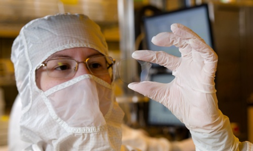
 A project at ETH Zurich and the Swiss Federal Laboratories for Materials Science and Technology (EMPA) has developed a new perovskite image sensor for machine vision and other applications.
Described in Nature, the semiconductor material is intended to improve colour reproduction and reduce image artifacts at lower light levels.
The goal was to tackle an inherent limitation of conventional silicon RGB image sensors in which the incoming light must be filtered, with pixels for specific colors using filters to block the other wavelengths. Each pixel thus only receives around a third of the available light.
At the ETH Zurich Functional Inorganic Materials Lab of Maksym Kovalenko, the project designed a solution based on lead halide perovskite, a material with semiconductor properties that can be adjusted through changes to the composition. If the perovskite contains slightly more iodine ions, it absorbs red light, while addition of bromine and chlorine improves sensitivity to green and blue respectively.
This means that the pixels for red, green and blue can be stacked on top of each other in the image sensor, rather than arranged side by side as in a conventional silicon sensor, and so capture more light compared to a sensor of the same surface area. Spatial resolution should be boosted by this stacked arrangement.
Smaller pixels from perovskite than silicon
Perovskite image sensors are still in the early stages of development, noted the project, with recent versions of multilayer sensors limited to mechanical stacking of three individual detectors. Practical implementations for real-world image sensor arrays will need monolithic thin-film stacking arrangements instead.
The project has now manufactured two prototypes using industry-standard thin-film processes, to demonstrate that its design can achieve the vertical dimensions needed for real-world applications. The key manufacturing choices involved all-evaporated perovskite layers and judicious choice of transport and dielectric materials, according to the team's Nature paper.
"We are developing the technology further from a rough proof of principle to a dimension where it could actually be used," said Maksym Kovalenko.
In trials, the two prototypes proved to be more sensitive to light, more precise in color reproduction and offered a significantly higher resolution than conventional silicon technology, according to the project. The fact that each pixel captures all the light also eliminates some of the artifacts of digital photography, such as demosaicing and the moiré effect.
"Demosaicing is a critical digital-image-processing technique, interpolating the missing colors for each pixel by analyzing the colors captured by adjacent pixels," said the team in its paper. "Stacked-perovskite detectors and other stacked-type sensors do not need demosaicing, as they capture complete colour information at every pixel location."
Machine vision and hyperspectral imaging could both benefit from the stacked perovskite technology, thanks to precise control of the wavelength range absorbed by each layer in the sensor.
The project now aims to both reduce the sensor size further and increase the number of pixels. The two prototypes had pixel sizes between 0.5 and 1 millimeter, while commercial image sensors fall in the micron range. Once optimized, the new approach could reduce pixel size below that level.
"It should be possible to make even smaller pixels from perovskite than from silicon," commented Sergii Yakunin from ETH Zurich.
Exail poised for Thales takeover
July 13 2026
Magic Leap pivots to AR waveguide supply
July 13 2026