Horizon2020-supported HIOS sensor project completed
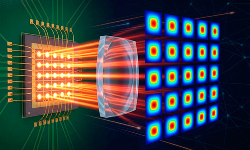
First light sensor with optical stack, multiple filters, lenses; aperture replaces separate components.
28 November 2019 Research & Development
 Sensor developer AMS, the coordinator of the Highly Integrated Optical Sensors (HIOS) research consortium has announced the successful completion of this novel optical senosr R&D project.
The HIOS consortium has developed and launched what it is calling "the world's first light sensor with fully integrated optical stack including multiple filters, lenses and an aperture replacing multiple discrete components."
Funded to the tune of €3 million under the Horizon2020 Grant Agreement (Fast Track to Innovation), the total-cost €4.3 million HIOS project has enabled AMS and its consortium partners - the process and equipment suppliers APC, Boschman and Bühler Leybold Optics - to "drive competitiveness in their respective markets."
Verena Vescoli, Senior VP, Research & Development, at AMS, commented, "Thanks to Horizon2020 funding from the European Union and collaboration from partners in the HIOS Consortium, we have been able to drive market innovation at a faster rate than would have otherwise been possible. This is a great example of how European companies can work together to compete on the world stage supported by the European Union."
HIOS consortium
The HIOS Consortium developers say the sensor, which incorporates 3D technology, IC filter and wafer level optics integration technologies, "is also expected to bring further cost-efficient, small, and high-performance sensors to the market."
AMS established a high-volume production environment for 3D/Through Silicon Via process technology which has now been extended by equipment and processes for on-chip inorganic optical filters and wafer level molding to form on-chip optical components.
Departing from the initial concept for an ambient light sensor, the project focused on enabling the later launch of a wavelength sensor as an achievable target. AMS explained that to reach this shared goal, "All partners had to push the boundaries of capabilities in their fields while cooperating seamlessly at the same time."
Bühler Leybold Optics developed and enhanced new equipment for advanced optical interference filter processing and announced its new deposition tool for high performance optical coating, HELIOS Gen II, back in February 2019.
New hardware and PARMS+ process lead to a tighter specification with high productivity and yield. Boschman successfully established a higher level of accuracy with its molding tool and process development for optical packaging applications being capable to form diffusor layers, lenses and apertures.
As planned, all these developments were successfully demonstrated for implementation on the AMS range of ambient light sensors products. Based on the interference filters developed throughout this project, new spectral color sensor products could be designed covering applications from UV, visible and infrared wavelengths.
AR Alliance grows as Meta launches prescription eyewear
April 01 2026
Monarch lands $55M for ‘quantum light engines’
April 01 2026
Lumentum to scale InP lasers at new US fab
April 01 2026


