|

11 Jan 2006
High-end cooled digital cameras featuring electron multiplying CCD technology are revolutionizing our ability to image very weak photon fluxes successfully, says Colin Coates.
Continual advancements in imaging and spectroscopy are placing unprecedented demands on camera technology to perform at significantly higher levels. Techniques such as intracellular ion signalling microscopy (e.g. Ca2+ flux microscopy) and multidimensional (4-5D) microscopy on live cells impose considerable demands on detection technology, in terms of higher sensitivity at faster frame speeds. Electron multiplying charge-coupled device (EMCCD) camera technology has been designed to respond to this growing need.
The development of the EMCCD is heralding a new era of low-concentration chemical analysis, which was previously not possible. For example, the behaviour and interactions of individual biomolecules can now be tracked at exceptionally rapid frame rates, even within their natural cellular environment. Similarly, Raman spectroscopy, astronomy and neutron tomography are benefiting from enhanced sensitivity at shorter exposure times.
EMCCD technology was first introduced to the digital scientific imaging community in 2001. It is an innovative approach for amplifying very low light signals above the read noise floor of the CCD, which usually sets the detection limit of the system. The approach harnesses the full quantum efficiency (QE) of the silicon sensors, in contrast with the intensifier tubes of ICCDs, which fundamentally restrict QE and have limited resolution.
Essentially, the EMCCD is an image sensor that is capable of detecting single-photon events, thanks to a unique electron-multiplying (EM) structure built into the chip. EM gain can be increased linearly and tuned in real time via software. It allows extremely weak signals to be detected above the read noise of the camera, at any read-out speed.
Traditional high-sensitivity CCD cameras offered high sensitivity with read-out noise in single figures below 10 electrons, but at the expense of slow read-out. Therefore they were often referred to as "slow scan" cameras. The fundamental constraint came from the CCD charge amplifier. To have high-speed operation, the bandwidth of the charge amplifier needs to be as wide as possible, but it is a fundamental principal that the noise scales with the bandwidth of the amplifier, and therefore that higher-speed amplifiers generate greater noise.
Slow scan CCDs have relatively low bandwidth and hence can only be read out at modest speeds of typically less than 1 MHz. EMCCD cameras avoid this constraint by amplifying the charge signal before the charge amplifier and thereby maintain unprecedented sensitivity at high speeds. By amplifying the signal, the read-out noise is effectively bypassed and is no longer the limit on sensitivity.
Device structure
Most EMCCDs utilize the frame-transfer CCD structure shown in figure 2. Frame-transfer CCDs feature two areas: a sensor area, which captures the image, and a storage area, where the image is stored prior to read-out. The storage area is normally identical in size to the sensor area and is covered with an opaque mask, usually made of aluminium. During image acquisition, the sensor area is exposed to light and an image is captured. This image is then automatically shifted downwards behind the masked region of the chip and then read out.
While the image is being read out, the sensor area is again exposed and the next image is acquired. The aluminium mask therefore acts like an electronic shutter. To read out the sensor the charge is shifted out through the read-out register and into the multiplication register, where amplification occurs prior to read-out by the charge amplifier.
The amplification occurs in the multiplication register (figure 2), which consists of many hundreds of cells. Each cell amplifies the signal by harnessing a process that occurs naturally in CCDs, known as clock-induced charge or spurious charge. Traditionally, clock-induced charge has been considered a source of noise and a phenomenon to minimize. However, in EMCCDs it is exploited for useful purposes. When clocking the charge through a register there is a very tiny but finite probability that the charges being clocked can create additional charges by a process known as "impact ionization". This occurs when a charge has sufficient energy to create another electron-hole pair and hence a free electron charge in the conduction band can create another charge and amplification occurs.
To make this process viable, EMCCDs tailor the process in two ways. First, the probability of any one charge creating a secondary electron is increased by giving the initial electron charge more energy by clocking the charge with a higher voltage. Second, the EMCCD is designed with hundreds of cells in which impact ionization can occur and, although the probability of amplification in any one cell is small, over the entire register of cells the probability is very high with gains of thousands achievable.
EMCCD cameras basically come in the same varieties as regular CCDs so they share the same properties and quantum efficiencies. While EMCCDs eliminate the real noise floor and render the detector single-photon sensitive, the amplification process adds additional noise, which must be taken into consideration, and results in a noise factor of greater than 1.
The EMCCD gain also complicates the dynamic range of the camera: initially, as the EM gain is applied, the dynamic range increases. The EM gain reduces the effective read noise but the higher well capacity in the EM gain register can accommodate the amplified signal. When the EM gain register can no longer accommodate the amplified full-well capacity of a pixel, the dynamic range flattens. When the gain is sufficient to reduce the noise below single-photon levels, the dynamic range then falls off.
The ultimate in sensitivity comes in the form of the back-illuminated EMCCD camera technology, which provides the maximum possible QE across the visible and near-IR wavelength range (> 90% at peak), enabling the detection of very small signals.
Applications
EMCCD technology is particularly suited to optical experiments with low photon levels. For example, it is a common choice for single-molecule detection experiments, typically using total internal reflectance fluorescence microscopy for parallel studies of single-molecule dynamics under reduced excitation power. The ability to detect single molecules in such a fashion has catalysed the race to develop a method that can sequence the entire human genome in less than 24 h.
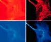
Live-cell fluorescence microscopy (including calcium flux, time-lapse, cell motility, and 4 and 5D confocal microscopy) has benefited enormously from this ultrasensitive technology. Improved camera sensitivity enables the use of shorter exposure times, while rapid synchronous shuttering enables one to achieve higher temporal resolution through multiple dimensions. These features allow the capture of more images before the cells succumb to phototoxicity or photobleaching.
The EMCCD is also suited to detecting intracellular bio- and chemiluminescence. These applications use no excitation source and so harness the true single-photon sensitive nature of the detector without fear of masking the signal with background photons. Under such circumstances, cooling becomes critically important and, if photon flux is very low, high signal-to-noise images can be attained through use of longer exposure times.
Recently, EMCCD technology has turned its attention to spectroscopy. The very weak signals inherent in most Raman applications require highly sensitive cameras.
Optimizing EMCCDs
To harness EMCCD technology effectively, a number of key parameters must be addressed and optimized during camera design to deliver a truly high-end system. The pioneering iXon camera platform from Andor Technology was designed from first principles to maximize the potential that this new technology promised.
An area that requires particular attention for optimizing EMCCD performance is that of thermoelectric (TE) cooling. By housing the sensor into a hermetically sealed, permanent vacuum enclosure, designed for minimal outgassing (rather than the lower-end approach of an o-ring-sealed, gas-filled housing), it is possible to achieve significantly lower temperatures. Enhanced cooling performance is a critical issue with EMCCD technology, because thermally generated electrons are amplified above the read noise floor, just as photoelectrons will be. It is thus crucial to minimize dark current as far as possible, even under rapid frame rates.
Another significant advantage of a permanent vacuum head is the protection that it gives the sensor from moisture and condensation. In fact, this approach enables removal of a window from the front of the sensor that is otherwise required for vacuum protection, resulting in increased throughput of the signal. Also, removing convection from the sensor enclosure eliminates the possibility of condensation on the outside of the front window.
Another parameter of EMCCD performance that requires considerable attention is charge shifting. It is beneficial in a frame transfer device to offer the ability and flexibility to push vertical clock times as fast as possible, thus minimizing smearing under short exposure times and increasing frame rate. The challenge comes in doing this while retaining the essential sensitivity performance, because a form of spurious single-electron noise called clock-induced charge is particularly sensitive to clock conditions. It is through careful optimization of voltage clocking parameters that the EMCCD can be operated successfully under these more challenging conditions.
 |  |  |  |  |  |  |
| © 2026 SPIE Europe |
|