 |
Date Announced: 01 Feb 2013
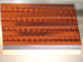
At SPIE BiOS 2013, Jenoptik is presenting high-index gallium phosphide microoptics for near to mid-wavelength infrared applications.
Microlenses, microlens arrays, and diffractive optics are used in medical applications for homogenization of laser beams for laser eye surgery and aesthetic skin treatment, for creating multi-spot arrays for ophthalmic diagnostics, for collimating and shaping laser beams for surgical applications, and for imaging applications such as optical coherence tomography and scanning confocal microscopy.
Recent advances in near infrared (NIR) and mid-wavelength infrared (MWIR) quantum cascade
and fiber lasers in conjunction with new diagnostic and treatment approaches are placing new demands on microoptics for these applications. These needs include a broad NIR - MWIR transmission, high numerical aperture (NA), and small form factor for minimally invasive applications. With 15 years of experience, Jenoptik´s Grayscale lithographically fabricated gallium phosphide (GaP) microlenses and microlens arrays meet these demands with:
1) A unique and broad wavelength range from 600 nanometers to beyond 5 mikrometers
2) A high refractive index of 3.1 allowing a single element lens or lens array with NA’s
up to 0.85
3) Complex surface shapes providing for beam collimation and circularization of high divergence diode lasers with a single element
Scanning confocal microscopy and minimally invasive optical coherence tomography are two examples where a single GaP microlens or microlens array can be used to extend the wavelength range over traditional GRIN and Si lenses. Jenoptik’s ability to fabricate complex aspheric elements with high numerical aperture also provide for better imaging performance when compared with GRIN lens based systems.
In addition, standard manufacturing processes are available for a range of different optical materials such as SiO2, GaAs, CaF2, Al2O3, ZnS, ZnSe, Ge, and chalcogenide glass.
Visit us at SPIE BiOS 2013, from February 2nd to 3rd, in San Francisco at the Moscone Center, south hall in booth # 8628.
About the Jenoptik Optical Systems division
Through its Optical Systems division, the Jenoptik Group delivers world-class precision optics and systems designed and manufactured to the highest quality standards.
Besides offering customized systems, modules and assemblies, the Optical Systems division is a development and production partner for optical, microoptical and coated optical components - made of optical glasses, IR materials as well as polymers.
It possesses outstanding expertise in the development and manufacture of optics and microoptics for beam shaping used in the semiconductor industry and laser material processing.
The product portfolio also includes optical and opto-electronic systems and components for applications in defense & security, health care & life science, digital imaging, machine vision as well as lighting.
E-mail: ines.schindler@jenoptik.com
Web Site: www.jenoptik.com/microoptics
| © 2026 SPIE Europe |
|