 |
Date Announced: 27 Nov 2012
SCHOTT developers are extending nanoimprint technology and opening the door to a whole world of applications.
Mainz, November 27, 2012 – The SCHOTT technology group has developed a nanostructuring technique for surfaces that already ranks among the important emerging technologies: so-called nanoimprint lithography. This technological platform should provide the basis for a wide range of innovative applications including decorative stainless steel appearances for glass, OLED applications and even photonic crystals.
Complex functional surface structures can be produced using nanoimprint lithography, a mechanical nano pressing technique, but also in combination with special coating materials and processes. These range even into the nanometer region – in other words one billionth of a meter – and are so sophisticated that they can systematically guide, reflect, absorb or manipulate incident light. They can also be used to produce surfaces with special textures or decorative appearances.
“We are working hard to turn nanostructuring into a technology platform for the future development of innovative applications and products,” says Dr. Eveline Rudigier-Voigt, Senior Manager for Coatings at SCHOTT Research & Technology. This technology was previously confined to industrial settings and relatively large surfaces and usable only with flexible substrates, primarily plastics.
Rigid materials such as glass allowed only small-scale structuring – nanostructured wafers or diffractive optical elements (DOEs), for example, as the successors to traditional lenses and mirrors. In addition, conventional processes are very slow, require many process steps, or are not suitable for large surfaces or rigid substrates such as special glass.
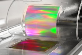
By contrast, an initial technological prototype from SCHOTT permits not only glass nanostructuring, but also rapid production of 30 cm x 40 cm glass formats. SCHOTT has also applied the principles of chemical nanotechnology to develop a special sol-gel based nanoimprint coating.
Applied to a glass substrate, this coating accommodates a wide variety of features, such as a customized refractive index for optical applications. In addition, these structures are very temperature-resistant and can withstand temperatures of over 200 to 700 degrees Celsius.
“This technology platform opens the doors to a wide variety of possible applications. We have secured broad patent protection for our materials and processes that will cover numerous applications,” comments Dr. Matthias Bockmeyer, SCHOTT Senior Manager on Material Development.
Other possible applications include architectural glass with special anti-reflective surfaces, holograms for product trademark protection, and optical nanostructures for light emission on OLEDs (organic light-emitting diodes).
Diffusion filters that distribute light more evenly on video screens are another option. Optical “light-trapping” concepts for more efficient absorption of light by the nanostructured substrate could also be an interesting application for thin-film solar technology.
Special crystalline silicon structures for producing photonic crystals more cost-effectively in order to boost (optical) data processing power – a prerequisite for the optical supercomputer of the future – represents yet another future field.
At SCHOTT, developers are already thinking about a decorative application for household appliances: the creation of a realistic brushed stainless steel look on glass. This would allow for the advantages of glass, such as easy cleaning and scratch resistance, to be combined with the elegant, stylish look of metal.
Source: Schott
E-mail: christine.fuhr@schott.com
Web Site: www.schott.com
| © 2026 SPIE Europe |
|