 |
Date Announced: 30 Aug 2012
ContourGT-X Analyzes Critical Yield Issues in Copper-based Processes in Semiconductor Packaging
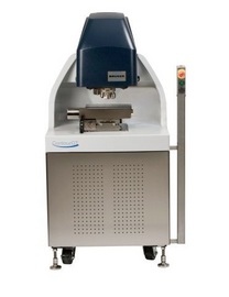
TUCSON, Ariz.--(BUSINESS WIRE)--Bruker announced today that a leading semiconductor supplier has purchased multiple Bruker ContourGT-X 3D optical microscope systems for their packaging factories in Asia and North America to support copper wire bond inspection and process control needs.
The production-level speed of the ContourGT-X, combined with its ease of use and custom production interface, can lower manufacturing costs and assists in solving critical problems impacting the entire semiconductor industry as it transitions to copper-based processes from more expensive gold-based processes.
“Since copper is harder and more brittle than gold, our customers need to precisely monitor the correct amount of force applied to the bond connecting the die to the package lead-frame or substrate,” said Mark R. Munch, Ph.D., President of the Bruker Nano Surfaces division. “This multiple-system purchase shows that the combination of automated run-time metrology, robust data analysis and ease of use for the operators is being recognized as a good solution for labor, process and material cost savings in Cu-wire bond qualifications.”
“In addition to the inherent 3D optical metrology advantages of the ContourGT-X, we have added a lot of features that are specifically designed to aid wire bonding applications,” explained Rob Loiterman, Executive Vice President and General Manager of Bruker’s Stylus and Optical Metrology business. “For example, a line engineer can create specific recipes that are automatically linked via operator ID, material ID, or lot/inspection ID. These software controls provide accurate real-time identification and flagging of good and bad product so our customers can ensure the reliability of their products, while taking advantage of the lower cost of copper.”
About the ContourGT 3D Optical Microscopes
The ContourGT 3D optical microscope family features patented, higher brightness dual-LED illumination that, when combined with the systems’ superior vertical resolution, greatly improves sensitivity and stability. These surface profilers enable precision non-contact 3D surface metrology in difficult applications and environments that are challenging for competing systems. The ContourGT microscopes also feature new Vision64™ operating and analysis software and the industry’s most intuitive, modular user interface to deliver user-level customization capabilities for a wide range of surface metrology applications.
Source: Bruker
E-mail: via web site
Web Site: www.bruker-nano.com
| © 2026 SPIE Europe |
|