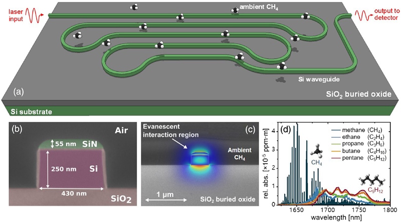
| The 'paperclip' geometry of the silicon waveguide (a, b) is chosen for its spatially efficient design, occupying only 16 mm2 but helping to boost the methane encountered by the evanescent field (c). Gas absorption spectra are shown in (d). Image: IBM/OSA. |
| © 2026 SPIE Europe |
|