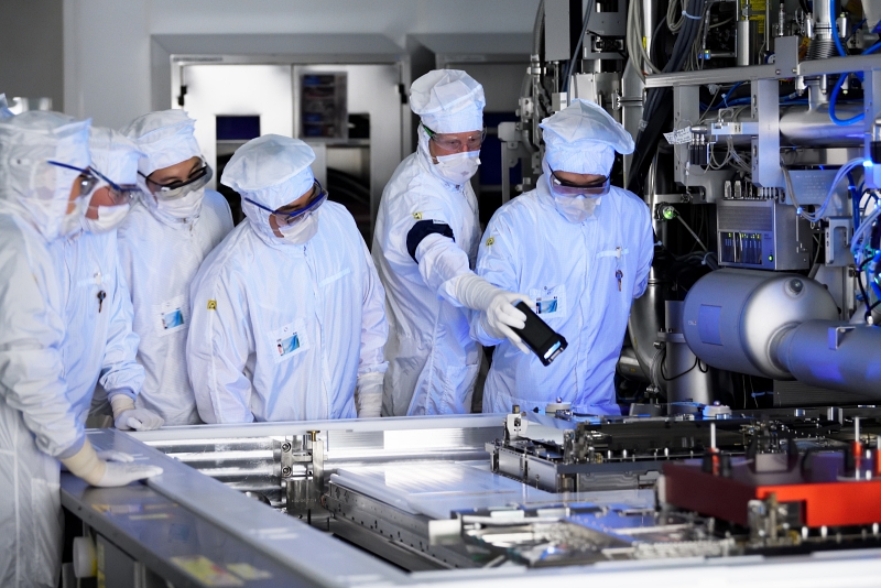
| EUV training at ASML: the company has a monopoly on the cutting-edge systems for making the latest chips, having spent billions developing the laser-based technology over the past couple of decades. It is now reaping the rewards of that investment, and working towards the next generation of systems, which will use high numerical aperture optics to further shrink the size of features that can be patterned on silicon wafers. Photo: ASML. |
| © 2026 SPIE Europe |
|