My Company
|
Advertise
|
Contact Us
daily coverage of the optics & photonics industry and the markets that it serves
Featured Showcases
Photonics West Showcase
News
Home
News
Latest News
Business News
Applications
Research & Development
Photonics World
Historical Archive
Notices
Press Releases
White Papers
Webinars
Products
Buyers Guide
Company Names
Optical Components
Laser Sources
Imaging & Detectors
Optical Test & Measurement
Laser Optics & Accessories
Software
Non-laser Light Sources
Optical Materials
Fabrication & Assembly
Vacuum
Media & Marketing
Jobs
Employers
Events
Publications
Newsletter
Product Focus
Vision Focus
AR/VR/MR Focus
Quantum Focus
Optatec Focus
Photonex Review
Show Daily
Photonics Focus
Advertise
Advertise
Resources
Return to article
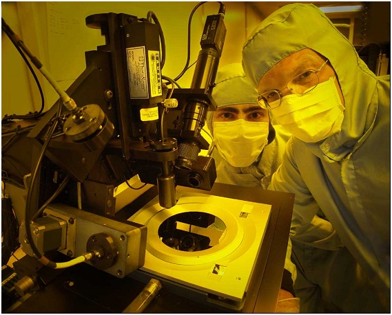
Researchers at the Australian National University's Laser Physics Centre in Sydney, Australia, map semiconductor wafers using a Filtek 4000 optical metrology tool from Scientific Computing International. Credit: ANU.
© 2026
SPIE Europe
Top of Page