 |
Date Announced: 16 Jun 2021
In response to increased demand for optics and sensors from semiconductor industry.
Prerov, Czech Republic -- Meopta has announced a major planned extension of production and R&D capacity in response to the highly increased demand for optics and sensors from semiconductor industry.
With more than 80 years of experience in the production of the most precision optics and as one of the world’s leading development and production partners for optical and optomechanical systems with the highest quality standards, Meopta is heavily involved in the development and introduction of future lithography technologies for semiconductor applications.
Meopta is growing and expanding its development and production capacities to ensure maximum customer support across the spectrum, but primarily with a focus on the heavily growing semiconductor industry. In line with the company's strategic intentions, significant investments were approved in order to build new and strengthen existing capacities for the production of optomechanical subassemblies used in semiconductor applications.
Impact of digitization
“Semiconductor manufacturers all around the world are investing in the extension of their production capacities in response to heavily increased demand due to digitization of almost every area of our life. Meopta with its strategy and planned investments is preparing for further growth and strengthens its position on a very competitive market as a realiable and valued supplier,"says Pavel Stastny, Business Unit Director for Industrial Applications.
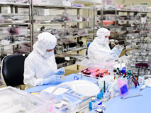
At Meopta, we value each Business Partnership and take it as a strong supplier-customer relationship, where the supplier always offers its customers the most efficient and comprehensive solutions tailored to their needs. It is the streamlining and improvement of production processes that will enable Meopta to build a new production space with an area up to 30,000 m2 designed mainly for the production of optical and mechanical components, which are the main building block of the optomechanical assemblies used in the semiconductor industry. These are and will be finally assembled in large new areas of clean rooms, where the cleanliness class meets the standards of ISO 4, ISO 5 and ISO 6 incl. AMC molecular purity levels.Innovation and production under one roof
Innovation and production under one roof
When designing the new production complex, we put a lot of emphasis on the flow material efficiency, which follows the current trend "Innovation and production under one roof", where it is possible to use modern logistics principles in a single-story building concept which guarantees reduced handling of individual components and increases the efficiency of the entire production process and thus the complexity of the final assemblies.
The concept of the production building is built to cover all production areas from the production of optics for wavelengths in the DUV range from sub-200nm to IR (spherical / aspherical, plane, cylindrical, phase optics, etc.) to the production of ultra-precision mechanical components.
E-mail: meopta@meopta.com
Web Site: www.meopta.com
| © 2026 SPIE Europe |
|