Optics.org
daily coverage of the optics & photonics industry and the markets that it serves
Featured Showcases
Photonics West Showcase
Press Releases
Menu
Press Release

EV Group launches next-gen step-and-repeat nanoimprint lithography system

Date Announced: 10 Jun 2021

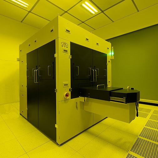
EVG 770 NT enables large-area fabrication of nano-structures for AR waveguides, optics, and biomedical chips.

ST. FLORIAN, Austria — EV Group (EVG), a leading supplier of wafer bonding and lithography equipment for the MEMS, nanotechnology and semiconductor markets, today announced the EVG®770 NT—its next-generation step-and-repeat nanoimprint lithography (NIL) system.
 
The EVG770 NT enables precise replication of micro- and nano-patterns for large-area master stamp fabrication used in high-volume manufacturing of augmented reality (AR) waveguides, wafer-level optics (WLO) and advanced lab-on-a-chip devices.
 
Until now, further developments and production scaling requirements for step-and-repeat NIL have often been limited by the availability of precise masters on larger areas. Leveraging EVG’s decades of experience in NIL and step-and-repeat mastering, the EVG770 NT has been designed as a fully production-oriented system to maximize performance, productivity and process controllability.
 
It provides industry-leading overlay accuracy and resolution with scalability up to 300-mm-wafer and Gen-2-panel sizes. As a result, customers can now realize the promise of high-volume, cost-efficient and high-fidelity NIL patterning.

Performance and scalability
The EVG770 NT includes several features that aid in both process development as well as production:

  • Stitchless replication of single lens/die templates up to 80mm x 80mm onto substrates up to
    300-mm wafers and Gen-2 (370mm x 470mm) panels
  • Sub-250-nm alignment accuracy and sub-50-nm resolution  
  • Enables a working-stamp high-volume-production process that avoids wear-out of the expensive original templates
  • A new exposure source design with higher dose that significantly reduces exposure times
  • Inspection microscopes and live process camera feeds to verify and monitor process results on the go
  • Non-contact air bearings to minimize particle contamination
  • Automated substrate loading and stamp changing unit with storage buffer for five stamps
  • In-situ control and characterization of imprinting and detachment forces
  • Software upgrade to EVG's latest Computer Integrated Manufacturing (CIM) Framework platform used across EVG’s high-volume-manufacturing process equipment

Product availability
The EVG770 NT has already been shipped to select customers and EVG is now accepting orders for the new system. EVG is also offering tool demonstrations and step-and-repeat mastering services on the new system at its NILPhotonics Competence Center at EVG’s headquarters. For more information on the EVG770 NT step-and-repeat NIL system, visit https://www.evgroup.com/products/nanoimprint-lithography/uv-nil-smartnil/evg-770/.

EVG at SPIE Digital Optical Technologies
EVG will present an invited paper on the benefits of NIL in manufacturing high refractive index waveguides at the SPIE Digital Optical Technologies Conference being held online on June 21-25, 2021.

Contact


Via website

E-mail: Marketing@EVGroup.com

Web Site: www.EVGroup.com

© 2024 SPIE Europe
Top of Page