 |
Date Announced: 22 Jul 2020
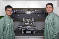
Two ORC researchers (Dr. Xia Chen and Dr. Milan Milosevic) are with the wafer-scale prober, which can autonomously and accurately perform optical and electrical device testing along with laser or electrical annealing.
ORC, Southampton, UK -- Power efficient and programmable circuit technology has been demonstrated in the Zepler Institute for Photonics and Nanoelectronics to bring silicon photonic applications to mass markets.
Scientists from the research institute's Optoelectronics Research Centre (ORC) have developed a method for making silicon photonics circuits that can be configured after fabrication for use in communications, computing or biomedical technologies.
A research team, including Dr Xia Chen, Dr Milan Milosevic and Xingshi Yu, led by Professor Graham Reed, have based the technique on integrated switching units that can be used as building blocks to create larger chip-based, programmable photonic circuits.
The approach expands the potential for silicon photonics technologies while also reducing production costs by allowing a generic optical circuit to be fabricated in bulk and then later programmed for specific applications.
Researchers have published their findings in The Optical Society journal Optics Express.
Single chip
Dr Xia Chen, Senior Research Fellow at the ORC, says: "Silicon photonics is capable of integrating optical devices and advanced microelectronic circuits all on a single chip. This new technology will have a wide range of applications. For example, it could be used to make integrated sensing devices to detect biochemical and medical substances as well as optical transceivers for connections used in high-performance computing systems and data centres."
The new research, which was funded by the Engineering and Physical Sciences Research Council, builds on earlier work in the ORC to develop an erasable version of an optical component known as a grating coupler. Scientists implanted germanium ions into silicon to alter the refractive index in an area, before a laser heating and cooling process could then reverse the refractive index and erase the grating coupler.
Researchers in the Silicon Photonics Group have now used the same technique to create components that can be applied to programmable circuits and switches. The journal paper reports that this is the first time sub-micron erasable waveguides have been created in silicon.
Cornerstone prototyping foundry
Waveguides, directional couplers, Mach Zhender interferometers, and two variants of switching circuits have been fabricated using the approach through the Cornerstone prototyping foundry, based in the University of Southampton's Mountbatten cleanroom complex, with photonic devices tested before and after programming with laser annealing demonstrating consistent performance. Since the publication of the paper in Optics Express, the group have now carried out a proof of principle experiment to show that electrical annealing of the erasable components is also possible.
The group are working with industry partners at ficonTEC to demonstrate a method for the annealing process to take place at wafer scale, so that hundreds or thousands of chips could be programmed automatically.
E-mail: light@orc.soton.ac.uk
Web Site: www.orc.soton.ac.uk
| © 2026 SPIE Europe |
|