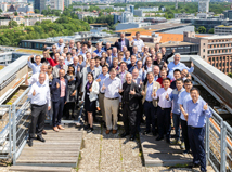
Fraunhofer HHI’s executive director Prof. Dr. rer. nat. Martin Schell opened the forum with a keynote in which he gave an overview of photonic integration approaches and discussed their dynamic economic potential. Over the course of three days, discussions were held, involving all the main platforms including Silicon Photonics, Indium Phosphide and Silicon Nitride as well as the tools and technologies concerning the production, packaging, assembly and testing of these next generation chips.
Professor Ton Backx, President of the Institute for Photonic Integration at Eindhoven University of Technology, believes that Indium Phosphide is going to be required in all roadmap scenarios. José Pozo, Director of Technology and Innovation at the European Photonics Industry Consortium (EPIC) focused also on solutions to real-world challenges in industries like automotive, healthcare, space and agri-tech.
However, as soon as new solutions for the photonics part are developed, the speed of the electronics becomes a severe bottleneck. Thus, industry specialists agree that a global approach to mapping is essential, if the photonics industry is going to successfully scale up. Shared manufacturing platforms and underlying standards for photonic integrated circuit design are key to cost-effective, high-volume manufacturing. This is going to be needed by emerging industries like 5G Telecom, next generation datacentres and a wide variety of smart “connected” sensors in healthcare and agricultural technology.
Until now, there are two very different but significant photonics roadmaps. One came out of Eindhoven University of Technology, Netherlands, the other from the MIT Microphotonics Center in Cambridge, USA. The WTMW 2019 in Berlin has been important to combine the two plans. They are meant to be combined into a single coherent Integrated Photonic Systems Roadmap-International. The further goal for coming years is to strongly improve the application side of the roadmap and align the technology roadmap to these application demands.
The results of the WTMF 2019 are available here. You can also find videos from the 10 keynotes, sector briefings, and the detailed outcomes of the workshops.


