 |
Date Announced: 30 Aug 2017
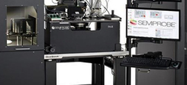
Helsinki, Finland -- VTT has acquired a system from SemiProbe to perform automatic and simultaneous Electro-Optical tests at Wafer Level (E/O WLT). The new and improved system will support both research and the SiPh production activities at VTT Memsfab.
The system, installed and operational at Micronova facility is able to handle 6"and 8" wafers and can be loaded with 2 full cassettes (25 wafers each) containing several hundred-thousands of E/O devices to test.
Test data are automatically acquired in customer-specified formats and let them available for analytics almost in real time, providing essential feedback and better understanding about production yield, process tuning needs or possible new chip design iterations.
The prober is also expected to work with a minimum level of surveillance during day shifts and be completely unmanned along the overnight shift, after loading operations.
"Leveraging on our expertise, we want to continuously improve the quality of complex testing services we are offering to our customers. We are excited to use this automatic probing station where we contribute applying our unique fiber probing and alignment know-how, allowing the machine to simultaneously probe each device optically and electrically (RF up to 50GHz)," said Giovanni Delrosso, Senior Scientist and Project Manager at the Photonics Integration team.
According to Timo Aalto, Research Team Leader, silicon photonics has been one of the fastest growing areas at VTT in the past few years.
"In 2016 we delivered thousands of SiPh chips for our customers. In 2018, the volume is targeted to reach more than 1 million tested chips", E/O Wafer Level Test is therefore vital in our R&D and manufacturing value chains," Aalto said.
E-mail: info@vtt.fi
Web Site: www.vttresearch.com
| © 2026 SPIE Europe |
|