 |
Date Announced: 11 Oct 2016
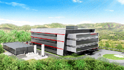
Miyakoda Factory new building no. 3 (exterior rendition).
Hamamatsu, Japan – Hamamatsu Photonics K.K. has announced the construction of a new building no. 3 at its Miyakoda Factory to increase manufacturing capacity of compound semiconductor devices. This expansion is being done in anticipation of growing demand for detectors and emitters in various applications that utilize infrared light.
A groundbreaking ceremony will be held on the site of the new building on October 12. Construction is scheduled to be completed in October 2017.
• The company last month announced that it has expanded the range of its Lightningcure LC-L5G linear irradiation type UV-LED units, designed for drying UV adhesives and UV coatings by introducing the new GC series.
The GC series features a thin profile, low power consumption, and a connectable structure that allows multiple units to be connected to cover wider printer formats. Applications of the GC series include UV curing in the manufacture of electronic devices such as televisions, tablets, and smartphones. The GC series is available from October 1, 2016.
E-mail: europe@hamamatsu.de
Web Site: www.hamamatsu.com/eu/en/index.html
| © 2026 SPIE Europe |
|