 |
Date Announced: 12 Nov 2010
MEMS structures fabricated using laser process.
Hamamatsu Photonics introduce a new range of silicon detectors and image sensors that offer enhanced near-infrared sensitivity. Using unique laser processing technology, MEMS structures can be fabricated on the silicon surface which act to reduce reflections and increase the surface area of the active element. This process drastically increases the sensitivity in wavelengths longer than 800nm.
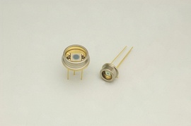
The S11518 and S11519 are silicon avalanche photodiodes (APDs) utilising this new technology, offering ultra high sensitivities at 1000nm, of between 70-75A/W at a gain of 100. Compared to conventional APDs designed for YAG laser detection, the S11518 and S11519 offer an additional 15-20A/W photo sensitivity, under the same operating conditions. At 1.06µm, the quantum efficiency of these new APDs reaches 40%, compared to 20% for a conventional APD.
Both the S11518 and S11519 are available in 1mm diameter and 3mm diameter active area types, which offer bandwidths between 220MHz and 400MHz. The S11519 is specially designed for low bias operation, with improved breakdown voltage, dark current and cut-off frequency characteristics compared to a conventional APD.
The increased sensitivity in the near-infrared region makes the S11518 and S11519 IR-Enhanced APDs suitable for a wide range of applications, including YAG laser monitors, high speed IR measurements, and many more.
Source: Hamamatsu Photonics
E-mail: info@hamamatsu.co.uk
Web Site: www.hamamatsu.co.uk
| © 2026 SPIE Europe |
|