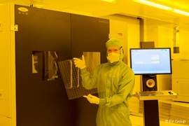
EV Group scales up nanoimprint lithography for display manufacturing
Date Announced: 14 Mar 2016
New EVG®7200 LA SmartNIL™ system brings high-resolution and low cost-of-ownership advantages to high-end displays, photonics, optics and biotechnology applications.
ST. FLORIAN, Austria, March 14, 2016--EV Group (EVG), a leading supplier of wafer bonding and lithography equipment for the MEMS, nanotechnology and semiconductor markets, today introduced the EVG®7200 LA SmartNIL™ system for display manufacturing and other applications that require large-area substrates. Leveraging EVG's proprietary SmartNIL technology, the automated UV nanoimprint lithography (UV-NIL) system enables cost-efficient nano-patterning in high-volume manufacturing (HVM) applications.
The EVG7200 LA is specifically designed for Gen 2 (370 mm x 470 mm) display panel manufacturing but can address a wide spectrum of biotechnology, photonics and optics applications. A few examples of imprinted patterns and devices supported by the EVG7200 LA include: wire grid polarizers, which enable better clarity and lower power consumption; lenticular lenses for direct-view 3D screens; and other functional surfaces that enable new features and specifications.
NIL is a highly cost-efficient method of enabling nano-scale patterns on large areas since it is not limited by sophisticated optics that are required with optical lithography, and since it can provide optimal pattern fidelity for extremely small (sub-100-nm) structures. EVG, which has the largest installed base of NIL systems in production, has continually extended the capabilities of its NIL solutions to address new and emerging market needs and technology requirements. The latest addition to EVG's NIL portfolio--the EVG7200 LA--brings nanoimprint lithography to a whole new level by enabling high-quality nano-patterning on panel-size substrates. As a result, novel structures based on nanotechnology that can improve device performance are now available for use in display manufacturing and other demanding large-area applications.
"EV Group's market and technology leadership in nanoimprint lithography is built on years of field experience working with our partners and customers in multiple markets, as well as research and development work in our demo labs and NIL Photonics Competence Center," stated Dr. Thomas Glinsner, corporate technology director at EV Group. "Driven by customer demand, we took our robust SmartNIL technology--which has already achieved outstanding imprint results on substrates up to 200 mm in diameter in high-volume manufacturing--and scaled it up to Gen 2 panel size. With the EVG7200 LA, we can now offer a full patterning solution for the display market, where companies have not previously considered NIL for their manufacturing efforts."
The EVG7200 LA features EVG's SmartNIL technology, which in combination with multi-use soft working stamp technology adapts to uneven and rough surfaces to provide unmatched conformal imprinting (down to 40 nm) with high uniformity and pattern fidelity. This capability is especially critical to successfully manufacture wire grid polarizers, where pattern transfer into metal layers is needed and where critical dimensions of the device features fall below 100 nm. In addition, SmartNIL's soft stamp fabrication technology combined with automated low-force detachment extends the lifetime of master stamps, which results in significant cost savings for customers.
Demonstrations of the EVG7200 LA SmartNIL system are available at EVG's headquarters in St. Florian, Austria.
Source: EV Group
Contact
via web site
E-mail: via web site
Web Site: www.evgroup.com
