Photon Bridge lands €10M to scale lasers for data centers
Dutch startup aiming to break AI ‘bottleneck’ with high-yielding approach reducing individual laser power requirement.
21 October 2026

Photon Bridge, a startup in Eindhoven, The Netherlands, working on a novel laser diode architecture designed to support much higher production volumes than is currently possible, says it has raised €10 million in a new round of venture funding.
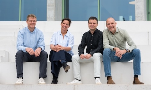
Founded in 2020 by company CTO Rui Santos and Xaveer Leijtens, an associate professor at Eindhoven's University of Technology, the firm believes that its approach can dramatically reduce manufacturing complexity while enabling higher bandwidth and lower-power optical engines.
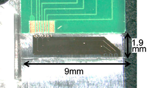
Key to that are the use of thick-film silicon photonics and a patented cantilever waveguide technology that has been purpose-built to bridge silicon photonics with any III–V material system.
The Photon Bridge team sees that as a solution to scaling up indium phosphide (InP) laser production to the levels that are expected to be required in the near future for AI data center interconnects.
“Today’s high-power laser supply chain was largely built for telecom and subsea networks, where volumes are far lower,” explains the startup. “AI could transform the laser from a specialist photonics component into something that has to be manufactured at semiconductor scale.
“Photon Bridge has designed its technology around that transition. Rather than generating the required optical power using a small number of increasingly powerful lasers, Photon Bridge combines and multiplexes light from multiple lower-power semiconductor lasers.”
Manufacturing challenge
One key advantage of that approach is that lower power densities make individual lasers less sensitive to manufacturing defects - enabling higher production yields at InP device foundries and a pathway to much higher volumes.
Photon Bridge’s platform is designed to deliver high wavelength counts with up to 40 mW of optical power per wavelength per fiber, while enabling production across multiple InP foundries.
CEO Paul Marchal added: “AI is fundamentally changing the way computing infrastructure is built. We are moving towards enormous systems in which hundreds of thousands of processors have to operate together, and moving data between them is becoming one of the defining constraints on performance.
“That means optics has to move closer to the compute. But it also creates an entirely different manufacturing challenge. The industry will soon need millions of these laser sources every year. Instead of making individual lasers increasingly powerful and difficult to manufacture, we move that scaling challenge into the architecture.”
Full passive alignment
According to the startup’s web site, the cantilever waveguide approach offers a universal interface enabling seamless integration of active devices including lasers, amplifiers, and modulators, onto silicon photonics interposers without the need for material-specific customization.
“The cantilever structures support full passive alignment of optical I/Os, transforming typical placement accuracies of [around] 2 microns into effective alignments of better than 200 nm,” it claims. “This precision delivers a high-performance, butt-coupled optical interface between III–V devices and the silicon photonics interposer, without active alignment or tuning.”
The technology is also said to enable optical I/O bonding to be performed simultaneously with standard electrical I/O flip-chip bonding, meaning that secondary optical attach steps are not needed.
“The robustness and repeatability of the assembly process delivers high manufacturing yields, making the number of optical I/Os per chip effectively unlimited and enabling true scalability for next-generation photonic systems,” adds the firm.
Providing the latest funding, which follows a €4.75 million seed round announced in January 2025, were new investors the Amadeus APEX Technology Fund and 360 Capital, with existing backers Innovation Industries, Faber, and the Brabant Development Agency (BOM) also taking part.
The money will be used to accelerate product development and customer qualification, with Photon Bridge expecting to deliver its first samples next year, and prepare for volume manufacturing from 2028.
MKS sells Ophir Optics division to PCB maker TTM for $650M
October 22 2026