



NIST scientists produce selectable-wavelength lasers in tiny circuits
Stacking dopants on fingernail-sized silicon wafers is new way to make optical chips.
22 April 2026
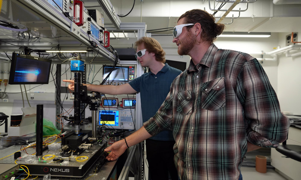
Lindell Williams (left) and Grant Brodnik align an optical fiber with the edge of an integrated photonics chip. Optical fibers act as pipes for light, enabling the light generated on these chips to be collected and routed off the chip for use in experiments and applications. Credit: R. Jacobson/NIST.
Computer chips that cram billions of electronic devices into a few square inches have powered the digital economy and transformed the world. Scientists may be on the cusp of launching a similar technological revolution — this time using light. Now the U.S. National Institute of Standards and Technology (NIST) has pioneered a way to make integrated circuits for light by depositing complex patterns of specialized materials onto silicon wafers. These photonic chips feature lasers, waveguides, filters and switches to process information.
Making circuitry for light as powerful and ubiquitous as circuitry for electrons is one of today’s technological frontiers, said Scott Papp, a NIST physicist whose group led the research, published this week in Nature. “We’re learning to make complex circuits with many functions, cutting across many application areas,” said Papp.
Several hurdles remain before integrated photonics can truly hit its stride, adds NIST. One involves lasers: high-quality, compact and efficient lasers exist in only a few wavelengths, or colors, of light. For example, semiconductor lasers are very good at generating infrared light with a wavelength of 980 nm.
Emerging technologies such as optical atomic clocks and quantum computers need laser light in many wavelengths. The lasers that produce those colors are big, costly and power-hungry, effectively confining these quantum technologies to a handful of special-purpose labs.
Multilayered approach
The new NIST photonics chip resembles a layer cake. NIST physicists Papp and Grant Brodnik, along with colleagues, started with a standard wafer of silicon coated with silicon dioxide and lithium niobate.
The researchers then added pieces of metal to electrically control how the circuits convert wavelengths. The scientists also created other metal-lithium niobate interfaces that allowed them to rapidly turn light on and off within the circuits — a crucial ability for data processing and high-speed routing.
On top of this was a second nonlinear material tantalum pentoxide, or tantala. Tantala can transform light into a full rainbow of visible light wavelengths plus a wide range of infrared wavelengths. Papp and colleagues have spent years developing techniques to fabricate circuits out of tantala without heating it up.
By patterning the different materials on top of each other in a three-dimensional stack, the researchers produced a single chip that efficiently routes light between layers. That allowed them to merge the light-manipulating wizardry of tantala with the controllability of lithium niobate. The new technique “allows seamless integration,” says Brodnik. “The real power is that tantala can be added to existing circuitry.”
Ultimately, the researchers were able to fit roughly 50 fingernail-sized chips containing 10,000 photonic circuits, each outputting a unique wavelength, onto a wafer roughly the size of a beer coaster. “We can create all these different colors, just by designing circuits,” said Papp.
Many potential applications
Quantum technologies such as clocks and computers could be among the biggest beneficiaries of integrated photonics. These devices often use arrays of atoms to store and process information. For each type of atom, physicists need lasers tailored to the atom’s internal quantum energy levels.
For example, rubidium atoms, commonly used in quantum computers and clocks, respond to red light with a wavelength of 780 nm. Strontium atoms, another popular choice, “see” blue light at 461 nm. Shine other colors on the atoms and nothing happens.
The bulky, costly and complicated lasers needed to produce these wavelengths have been a major hindrance to getting quantum computers and optical clocks out of the lab and into the field, where they could have big impacts. Cheap, low-power, portable optical clocks, for example, could help predict volcanic eruptions and earthquakes, offer an alternative to GPS for positioning and navigation, and help scientists investigate scientific mysteries such as the nature of dark matter. Quantum computers could offer new ways to study the physics and chemistry of drugs and materials.
Integrated photonic circuits are not just for quantum applications. Papp believes NIST’s photonics chips could help efficiently shuttle signals between the specialized chips used by tech firms, potentially making AI-based tools more powerful and efficient. Tech companies are also interested in using photonics to improve virtual reality displays.
While NIST’s chips are not yet ready for mass production, the technique used to create them provides a path forward, Papp and Brodnik say. The NIST scientists collaborated with experts at Octave Photonics, a Louisville, Colorado-based startup company founded by former NIST researchers that is now working to scale up the technology.




Tufts University observes Herpes virus reshaping neurons
August 26 2026