


ICFO’s chemistry advance takes quantum-dot IR detectors closer to market...
...and Tanaka develops lead-free precious metal quantum dot material.
11 November 2026
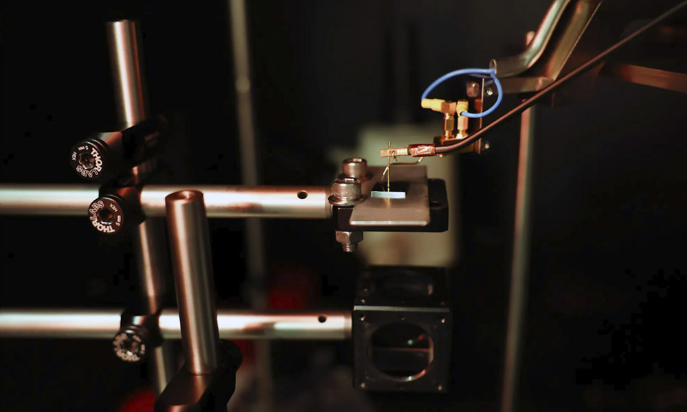
SWIR quantum dots at the laboratory. Using these, ICFO has built photodiodes with sensitivity comparable to commercially-available photodetectors. Credit: ICFO.
Scientists at Barcelona-based research center ICFO have developed a new chemical strategy to overcome a long-standing limitation of colloidal quantum-dots: electronic defects associated with their surfaces. With the treated dots, they have built photodiodes achieving sensitivity comparable to commercially available photodetectors, opening opportunities for a broader range of optoelectronic technologies. The study is published in Nature Communications.
Colloidal quantum dots are tiny semiconductor crystals whose optical and electronic properties can be precisely tuned by controlling their size. Unlike conventional crystalline semiconductors, they can be synthesized in solution and deposited onto different substrates using comparatively simple processing methods, and can be easily integrated with CMOS readout electronics. Their versatility, scalability and low cost makes them attractive building blocks for a wide range of technologies, from solar cells and light-emitting devices to infrared photodetectors and imaging systems.
However, despite decades of progress, quantum-dot semiconductors have struggled to match the electronic quality of their single-crystalline counterparts, such as indium gallium arsenide. One of the main reasons lies at their surfaces, where imperfect chemical bonding creates electronic defects that limit the final device performance.
The challenge becomes particularly pronounced in larger lead sulfide quantum dots, which are needed to absorb light at longer infrared wavelengths. As quantum dots grow, they expose different facets, including non-polar surfaces, which are difficult to protect using conventional chemical treatments.
Now, ICFO researchers Dr. Debranjan Mandal, Dr. Yongjie Wang, Dr. Carmelita Rodà, Dr. Miguel Dosil, Dr. Gaurav Kumar and Dr. Lucheng Peng, led by ICREA Prof. Gerasimos Konstantatos, have developed a new passivation strategy to neutralize surface defects that, instead of relying on traditional halide-based treatments, is based on metal-thiolate chemistry.
As demonstrated in a recently published Nature Communications study, thiolates enable more effective passivation of the non-polar facets of large PbS quantum dots, while also addressing their polar surfaces. Consequently, quantum dots exhibit substantially improved electronic quality and thermal stability compared with conventionally treated materials.
“For years, a central challenge in colloidal quantum-dot technology has been understanding why these materials, despite their attractive properties, still suffer from electronic losses that are much larger than those of conventional semiconductors,” said ICREA Prof. Gerasimos Konstantatos, senior researcher of the article. “We have now identified that incomplete passivation of non-polar quantum-dot surfaces is an important source of these losses.”
 Better materials, high-performance IR photodetectors, and more
To demonstrate the technological impact of their approach, the researchers incorporated the treated PbS quantum dots into short-wave infrared photodiodes. The devices exhibited exceptionally low dark currents and electrical noise, with performance substantially improved over previously reported SWIR quantum-dot photodetectors. Most notably, they reached sensitivity levels comparable to those of commercially available InGaAs photodiodes.
At the same time, this achievement has implications extending well beyond infrared detection. In particular, the new passivation strategy could improve the performance of quantum-dot photovoltaic technologies, where voltage losses remain a major limitation.
“What makes this result particularly important is that we are addressing a fundamental limitation of the semiconductor material, rather than simply optimizing a particular device,” said Dr. Debranjan Mandal, first author of the study. “The improvements in electronic quality and stability could thus benefit several quantum-dot technologies, including photovoltaics and infrared optoelectronics,” he said.
Overall, the study illustrates how advances in chemical control at the nanoscale can translate into improvements in semiconductor performance, bringing solution-processed quantum-dot technologies closer to the standards established by conventional crystalline materials. This could ultimately make SWIR photodectectors and other optoelectronic devices more widely available for industrial and commercial use.
Tanaka develops lead-free precious metal quantum dot material
Tanaka Precious Metal Technologies has developed a lead-free precious metal quantum dot material responsive to near-infrared light through joint research with the Torimoto Laboratory at Nagoya University, Tokai National Higher Education and Research System, all based in Japan. The new material offers a detection wavelength range comparable to that of conventional lead-based quantum dot materials while containing neither lead nor cadmium. The developer says that this “makes the material promising for use in consumer electronics such as smartphones and in medical fields such as biosensing.” Samples are scheduled to become available in January 2027.
 The new material is being presented at Okinawa Colloids 2026, from November 1 to 6, 2026, and at nano tech 2026, the 26th International Nanotechnology Exhibition & Conference, to be held in Tokyo from December 16 to 18, 2026.
Prof. Torimoto of Nagoya University commented, “this compound semiconductor quantum dot material is composed primarily of precious metals and is sensitive to infrared light. Like other quantum dot materials such as PbS, it requires no vacuum process and can be deposited using printing processes suitable for large-area production. It is therefore expected to simplify the manufacturing process and reduce process costs.”
In performance evaluations conducted by Tanaka, the newly-developed silver-sulfur-tellurium (Ag-S-Te) quantum dots were incorporated as the active layer (photodetection layer) in a simple photosensor, which achieved a maximum external quantum efficiency of 18.4% for short-wave infrared light in the 1,200-1,700 nm wavelength range. This wavelength range is less susceptible to noise from sunlight and the effects of adverse weather, enabling high-precision sensing outdoors. Light in this wavelength range also offers greater eye safety and readily penetrates materials and biological tissue.
This development is expected to enable practical applications across a wide range of fields where the adoption of high-performance infrared sensors has previously been limited by cost and lead restrictions. These include consumer electronics such as smartphones (3D sensing for facial recognition and other functions), automotive lidar, industrial inspection cameras, and biosensing.

Optics11 secures €50M for expansion
November 11 2026


nLight still hampered by optics supply chain
November 10 2026

Chip industry momentum boosts Jenoptik order book
November 10 2026

University of Tokyo captures new details of cell organization...
November 10 2026