



ASML partners on 6-inch InP project in Europe
Semiconductor equipment giant aiming to help create integrated photonics ‘unicorn’ in Eindhoven.
25 June 2026
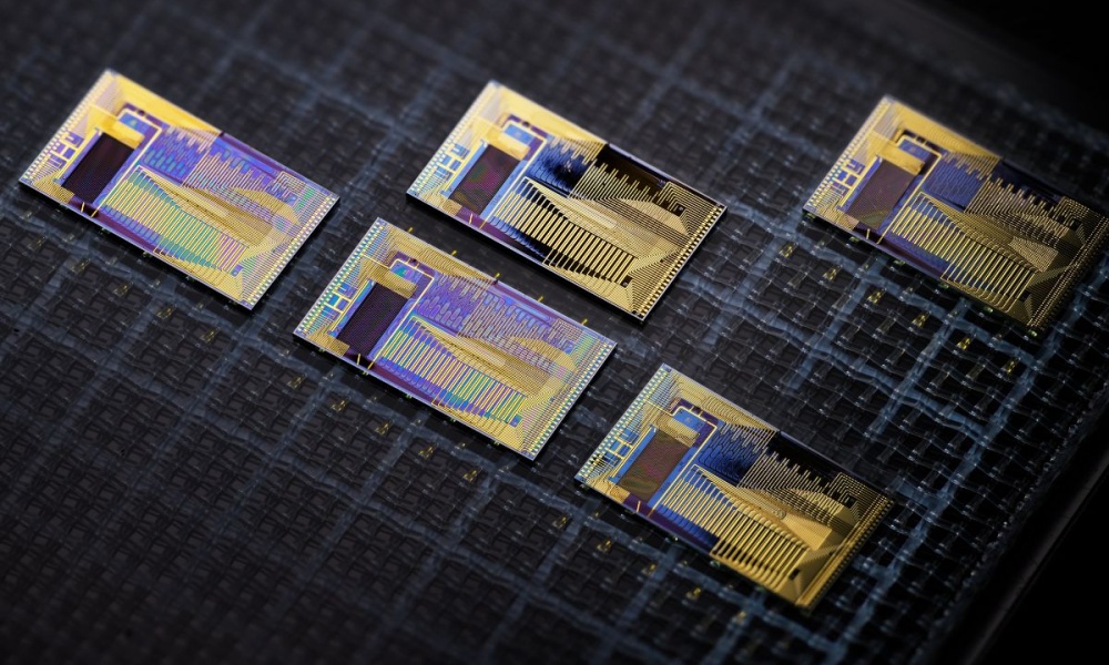
TNO and ASML are aiming to create a European 'unicorn' by establishing intergated photonics production on six-inch InP wafers at TNO's High Tech Campus in Eindhoven. Image: TNO.
ASML, the world’s key provider of lithography tools that are fundamental to the silicon semiconductor industry, has signed up as a partner on a European effort aiming to scale production of integrated photonics fabricated on indium phosphide (InP) wafers.
The collaboration will take place at TNO’s new pilot line for photonic chips, which is currently under construction at the High Tech Campus in Eindhoven, The Netherlands, a key hub in Europe for integrated photonics development.
News of the tie-up comes as US-headquartered Coherent and Lumentum each look to scale device production on six-inch diameter InP material - a shift in scale seen as critical to ensuring cost-effective fabrication of devices to be deployed in state-of-the-art data center interconnects that TNO also wants to establish as a sovereign capability in Europe.
“By aligning their technical expertise, the parties aim to enable scalable, high-volume manufacturing of photonic chips through lithography, process control, and metrology solutions,” announced the organization.
“The partnership involves a phased approach where ASML utilizes lithography equipment, including DUV and I-Line scanners, within the pilot line facility.
“This shared research and development environment facilitates technical workshops and joint innovation activities, allowing ASML to leverage TNO’s infrastructure for internal development and customer demonstrations.”
European unicorns
Arnaud de Jong, the managing director at TNO High Tech Industry, added: “This partnership with ASML reinforces our commitment to building European unicorns in the semiconductor landscape.
“By combining our R&D capabilities with world-class equipment, we are creating a unique pilot-line environment that will benefit the entire industry.”
Once operational, the InP fab is expected to facilitate full-scale manufacturing of advanced photonic chips at the six-inch wafer scale.
“Beyond physical manufacturing, the research ecosystem is already primed to leverage these advancements,” the partners announced. “TNO, Eindhoven University of Technology, and the University of Twente are working together within the jointly founded Photonic Integration Technology Centre (PITC) to turn innovative designs into real-world applications.
“This new structured collaboration with ASML is designed to improve operational performance and ensure Europe remains a global leader in the rapidly evolving integrated photonics landscape.”
Stanislas Baron, a senior VP at ASML, commented: “Scaling photonic chip technology requires a seamless transition from cutting-edge research to high-volume manufacturing.
”By integrating our lithography systems into TNO’s pilot line, we are bridging that gap. This collaboration gives us the ideal environment to optimize our processes for integrated photonics, ultimately accelerating the time-to-market for this transformative technology.”


Dissolving microneedles guide light to skin cancers
July 22 2026

Upbeat ASML raises 2026 guidance again
July 22 2026