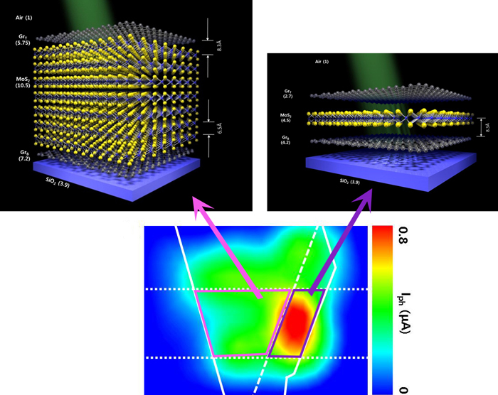
| (top) PV devices with one-layer and seven-layer MoS2 were built on top of a silicon base and compared. Dielectric constants responsible for the difference in electrostatic potentials are shown in parenthesis. (bottom) The device with one-layer MoS2 (in the violet box) showed better performance in converting light to electric current than the seven-layer device (in the pink box). Image: IBS. |
| © 2026 SPIE Europe |
|