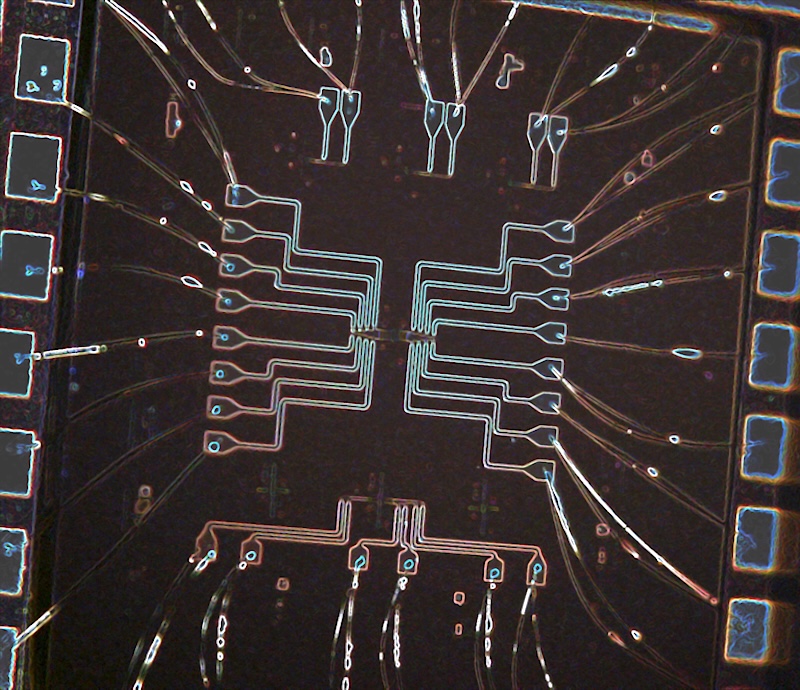
| An optical image of the electrically controlled coupled cavity array in the team’s silicon photonic chip. The image depicts the wiring structure and optical micrograph of the coupled cavity array. Credit: Abhi Saxena/University of Washington. |
| © 2026 SPIE Europe |
|