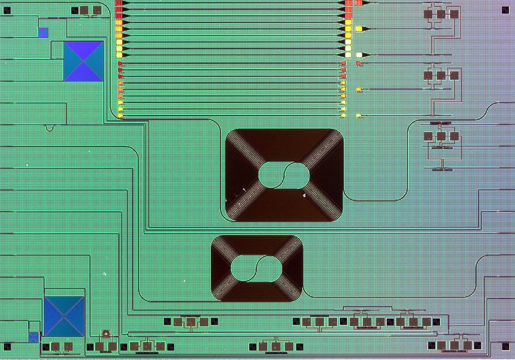
| Top-down view of the AIM/Spark Photonics 3rd generation active education and workforce development photonic integrated circuit (EWD PIC) chip as seen through an optical microscope at the Lab for Education & Application Prototypes (LEAP) facility located at Worcester Polytechnic Institute (WPI). The lab is a part of the LEAP Network, established by the Commonwealth of Massachusetts' M2I2 program to support AIM Photonics. (Photo courtesy of Worcester Polytechnic Institute) |
| © 2026 SPIE Europe |
|