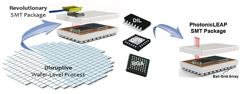
| PhotonicLEAP’s novel wafer-level PIC packaging and test technology will be used to produce a “revolutionary” Surface Mount Technology (SMT) PIC package, combining breakthroughs in advanced materials, innovations in optical and electrical packaging and ultra-fast wafer-level assembly processes giving >10 times reduction in PIC production costs. Graphic courtesy of PhotonicsLEAP program. |
| © 2026 SPIE Europe |
|