|

21 Jun 2002
Field-emission development has been struggling but some firms are still looking at hang-on-the-wall TV. Is it the beginning of the end or the end of the beginning?
From Displays Europe, May 2002
A few years ago, field-emission displays (FEDs) were held up as the likely replacement for CRTs in domestic TVs. The technology is similar to CRTs in that it lights screen phosphors with electron beams. A CRT uses a single-point hot electron source that is scanned across the screen to produce an image. FED pioneers such as Pixtech in France and Candescent in the US used an array of pointed microtips (so-called Spindt tips) that direct electrons at each pixel, allowing FEDs to be scaled down to a few millimetres in depth.
However, the similarity with CRTs ends there. Many pioneers found the technical hurdles too difficult to overcome and ceased development. This was the case recently with Motorola, and Sony and Candescent have pulled out of their joint development, leaving Pixtech as practically the only company persevering with Spindt tips and actually manufacturing products in any quantity (see photo).
But the company has no illusions about its technology taking over for TVs; it is targeting niche markets such as the automotive and medical industries. Said Bernard Bancal, Pixtech's director of R&D: "We have a 5.2 inch monochrome video device in production in Taiwan for instrumentation and ultrasound scan applications. We also have a 7 inch full-colour 16:9 aspect ratio pilot line in France for car applications such as navigation or rear-seat entertainment." Larger (up to 15 inch) displays are in development.
The 7 inch device is part of a long-standing collaboration with Audi, and Bancal says there could be full production in Taiwan some time this year. Pixtech also has a US operation, but was recently delisted from the NASDAQ index because of technical reasons concerning the share price, according to sales and marketing manager Martin Gallezot.
It is widely recognized that the future of FEDs is not in microtips, which suffer from a manufacturing point of view because of their small size (1-2 µm). An alternative is emission from flat surfaces up to 10 µm in diameter made from carbon nanotubes (CNTs) or some other combination of conductor and semiconductor. Motorola, for instance, abandoned microtip development last year, but it is still looking into CNTs.
According to Tim Harper, CEO of Spanish-based consultancy CMP-Cientifica: "The key to viable FED manufacture lies in moving to a simpler carbon-based structure. This allows the possibility of screen-printing cathode structures or simply using CNTs as emission sites."
Screen printing is the chosen route of UK-based Printable Field Emitters (PFE), which has ambitious plans to produce hang-on-the-wall TVs in the 20-40 inch range for a much lower cost than LCDs, organic LEDs (OLEDs) or PDPs (see graph and the item on PFE's technology entitled "The FED is dead: long live the FED" at the end of this feature).
One of the more exciting demonstrations of CNT technology happened at SID in Boston last month, when Ise Electronics of Japan described a 40 inch CNT panel. It will be the largest CNT display to date, and Ise hopes it will lead to hang-on-the-wall TVs by 2004. It is based on technology from FEPET of the US that Ise pioneered in a recent 14.5 inch prototype.
Critical nanotube price
An important factor in commercialization is the price of raw materials. A number of Japanese companies including Mitsui, Toray Industries and Mitsubishi Chemical have well advanced plans to mass-produce CNTs and bring prices down to ¥10 000 (€85)/kg.
Carbon Nanotechnologies (CNI), a spin-off of Rice University based in Houston, Texas, US, says it is bringing its CNT pilot plant online now. The company has an agreement with DuPont, which is now becoming ubiquitous in the FPD industry.
Said James Romine, director of material science at DuPont Central Research and Development: "The DuPont technology with laser-oven-produced CNTs will provide bright displays that operate at low voltage and consume a fraction of the power used by conventional TVs or PDPs."
SI Diamond of Austin, Texas, US, and its subsidiary FEPET, is also concentrating on carbon field emitters for slim wall-TVs, but on a larger scale than PFE - up to 150 inches on the diagonal.
FEPET is working on what it calls field-emission picture-element tubes (PETs) using carbon-film cathodes. The company's CEO Zvi Yaniv told Displays Europe that he was now driving the company to start manufacturing 10 mm pitch PETs for large wall TVs and advertising hoardings with Futaba of Japan early in 2003.
"There is a big vacuum of suitable direct-view displays in the 60-120 inch diagonal range," Yaniv said. "This is where I believe FEDs fit best. I have stopped believing that one technology can be the answer to all needs. I strongly believe that OLEDs (assuming that their stability problems are solved) will be very good for small displays, in particular for the portable market. I don't believe FEDs have a place in this market at the moment, but field emission will be an important player in very-large-area displays and will compete directly with plasma. This is what I am targeting with our technology and also with the HyFED development."
HyFED is a hybrid of the CRT electron optics technology and the carbon-emission film FED technology. It is simply an array of many small CRTs integrated together and enclosed in a common vacuum envelope in which the depth is dramatically reduced. Because each beam addresses many pixels, the number of drivers required is reduced by a factor of 10 compared with a standard FED device.
Other FED hopefuls who are dabbling in the field include Samsung with a CNT triode device, Matsushita and Hitachi using semiconductor-type processing, and Canon/Toshiba with surface-conduction emission, although no public statements have been made by Canon or Toshiba since 1999.
However, there are enough companies still in the field for FED technology not to be written off completely. To use Winston Churchill's immortal phrase at a crucial stage of the Second World War: "This may not be the end, it may not even be the beginning of the end, but it is the end of the beginning."
With additional reporting by Chris Chinnock.
*******************
The FED is dead: long live the FED
This was the title of the presentation given by Bill Taylor, technical director of PFE, to the DisplaySearch conference in San Diego, California, US, in March.
Practically the only company with an optimistic vision of the future of FEDs, PFE aims to produce devices with cheap screen printing processes. It has so far received £7.5 m (€12.2 m) from venture capitalists (the latest round in November 2001: £3 m from 3i, Quester and NIF). The company is also negotiating with Asian manufacturers for much larger funding.
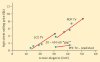
PFE's stated aim is to fill what it perceives to be the "20-40 inch gap" in the TV market. According to predictions by Stanford Resources for large display manufacturing costs, in 2010 LCDs will cost $1.5/inch2, tip-based FEDs will cost $1.3/inch2, and plasma and OLEDs will cost $1/inch2. Using the same model, PFE comes up with a cost of $0.5-$0.6/inch2. So, the PFE solution should be a third of the price of LCDs and half the lowest predicted for PDPs (see graph).
Taylor says that a printable FED at 32 inch would cost about $400 to make and would sell for around $1200; a 42 inch device would cost about $550 and sell for $1500-1800 in the shops.
PFE's latest prototype (see photograph) is being tested following the installation of a state-of-the-art etcher that provides greater process control. Full video-rate pictures without motion artefacts are now routinely being shown, says the company. Picture quality will also be further enhanced in the near future as two major technological enhancements are incorporated. Electronic compensation will be used to improve the uniformity from pixel to pixel, and a resistive ballast layer will enhance uniformity within each pixel.
*******************
 |  |  |  |  |  |  |
| © 2026 SPIE Europe |
|