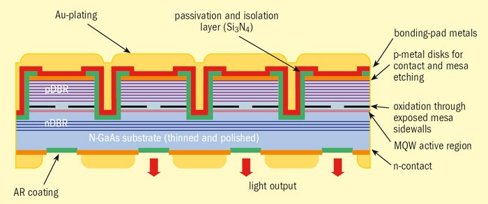
| Cross-section schematic of the processed VCSEL array. The GaAs substrate is thinned and polished to an optical finish, followed by the deposition of a quarter-wavelength Si3N4 layer (AR coating) and patterned evaporated metals to form the n-contacts and emission windows. Individual devices are defined by reactive-ion etching (RIE) of individual mesas followed by selective oxidation to form electrically conducting apertures. The p-contact disks serve as the RIE mask (self-aligned process). The epitaxial surface is then passivated with a Si3N4 layer. Windows are then opened by patterned etching of the nitride, followed by e-beam evaporation of Ti/Pt/Au metals to form the bonding pad. Both the n-metals and bonding pad are electroplated with gold to improve current distribution across the array. Credit: Princeton Optronics. |
| © 2026 SPIE Europe |
|