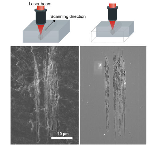
| SEM images of the entrance of the modified and etched channel directly after etching (left) and cross section of hollow nanoplanes in 500 μm depth of the same track. Laser beam propagated from top to bottom, three parallel scans with an offset of 3 μm, focused with NA=0.55, f=500 kHz, P=450 mW. Image credit: Optics Express/Dirk Wortmann. |
| © 2026 SPIE Europe |
|