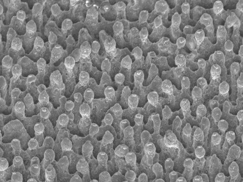
| Textured silicon: scanning electron micrograph showing the photodetector's laser etched surface. The microstructures are 2-3 microns tall and spaced at roughly 2-3 micron intervals. As the researchers explain, the shape of the pillars depends heavily on the laser fluence, shot number, gas species, gas pressure and pulse duration. (Credit: Harvard University, US) |
| © 2026 SPIE Europe |
|