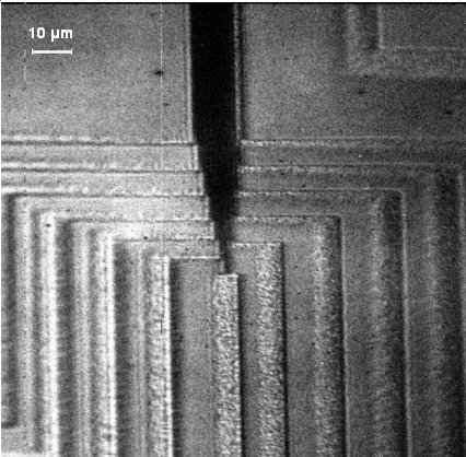
| The team put its EUV microscope to the test by imaging polysilicon lines patterned on a silicon wafer. The apparatus revealed features as small as 100 nm with an exposure time of only 20 seconds. (Credit: NSF ERC for Extreme Ultraviolet Science and Technology, US) |
| © 2026 SPIE Europe |
|