 |

09 Apr 2013
UK firm lands government support for dramatic capacity expansion, with roadmap targeting lighting-quality devices.
by Andy Extance
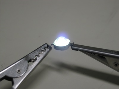
Plessey Semiconductors says that it has released the first LEDs manufactured on silicon substrates to be made commercially available anywhere in the world, with plans for a major capacity ramp in the works.
The Plymouth, UK, company is now sampling devices with a maximum luminous efficacy of around 45 lm/W and 75 mW maximum power, for applications including instrument panel backlighting and decorative lighting.
Plessey says that this is just the start of a technology roadmap that includes a ten-fold expansion of gallium nitride (GaN) material deposition capacity, something that would also establish the firm as the first volume producer of LEDs in the UK.
“This is the release of our first entry-level product,” Barry Dennington, Plessey’s chief operating officer, told optics.org. “Perhaps more significantly, as far as we know, it’s the first GaN-on-silicon LEDs that you’ll be able to buy in the market. Many more will follow quickly. We’ve visited our customers in the last couple of months with demonstrators of these products, and they are very excited by how far we’ve got.”
Competitive sector
While LED light bulbs are becoming more common, they remain expensive compared with both incandescent and compact fluorescent alternatives. To cut costs, many companies are hoping to swap the sapphire or silicon carbide (SiC) wafers upon which they normally deposit light-emitting GaN semiconductor material for silicon.
Silicon substrates are larger, offering economies of scale, and cheaper. And while 6-inch or 8-inch wafers represent the cutting edge in sapphire-based LED production, many fully depreciated silicon wafer manufacturing fabs could be repurposed to make the light emitters instead, and at minimal expense.
Major LED producers who are looking to exploit such advantages include Germany’s Osram Opto Semiconductors, which has worked closely with GaN-on-silicon specialist Azzurro Semiconductors. The Japanese electronics conglomerate Toshiba, which has close ties with US-based Bridgelux, said in December 2012 that it was starting to mass-produce 112 lm/W, 1 W, GaN-on-silicon LEDs.
However, Dennington underlined that Plessey does not believe that these devices have been made commercially available. “We have not been able to successfully acquire or find any GaN-on-silicon LEDs anywhere in the world,” he said.
While silicon substrates do offer a route to cheaper LED lighting, the approach still faces stiff competition from devices made on more conventional substrate materials. Just a month ago Cree, the vertically integrated US company that manufactures GaN-based LEDs on SiC material, launched a range of solid-state replacements for 40 W incandescent bulbs at a retail price just below $10.
Recipe for rebirth
Though a prestigious and historic brand in the world of electronics, Plessey is a far less familiar name in the LED and lighting markets, and the company will face huge challenges to compete with the LED lighting establishment.
Originally built in 1987, the Plymouth fab where the LEDs are produced became the first 6-inch VLSI CMOS line in Europe, before the fab was sold in 1998 following Plessey’s merger with GEC.
Through a series of ownership changes, the site’s engineers developed and maintained a relationship with the material sciences group at the University of Cambridge, which was developing GaN growth expertise.
Entrepreneur Michael Le Goff bought the Plymouth facility and combined it with other former Plessey assets under the firm’s original name in 2010. Shortly thereafter, Cambridge established a spin-out called CamGaN to commercialise its GaN-on-silicon growth expertise.
By February 2012, Le Goff had negotiated the acquisition of CamGaN too. “The university had the growth recipe,” Dennington explained. “We had the ability to apply integrated circuit capability to it: high volume, high quality, high throughput, high efficiency manufacturing.”
Though Dennington stressed the power of this combination, the growth recipe plays a critical role in making Plessey’s GaN-on-silicon LEDs competitive. It’s needed because silicon and GaN have different lattice structures and thermal expansion coefficients, meaning that after depositing GaN on silicon at 1000°C in a metal-organic chemical vapor deposition (MOCVD) tool, the LED wafers can flex and bow as they cool – an effect that is accentuated with larger wafers.
That can lead to cracked, unprocessable wafers, so LED makers must fight it. “As you grow GaN layers you add certain barrier layers that compensate and counteract any distortion, any bowing,” explained Dennington. “We have stopped the bow.”
While many approaches have been tried, Dennington claims that Plessey’s barrier layer recipe is superior. “The GaN growth is faster than other technologies, because the stack is thinner,” he said. “Our competitors are typically at 8 µm thickness: we’re at 2.5 µm, which means we can run our MOCVD reactor three times a day.”
Building belief
Plessey bought its first MOCVD reactor in August 2012, and commissioned it within three months, adding to its belief that it is leading the field. “From the experience with the tool supplier in bringing up the equipment, it’s clear to us that we’re definitely in the front,” Dennington said. The Plessey team has also developed its own lateral and vertical LED structures, as well as bonding and roughening process steps that help to maximize light output.
Such advances will be important as the company seeks to reach beyond its entry-level devices and release chips suitable for general lighting. “To get into lighting applications we need to be above 70 lm/W and we have a very clear roadmap into those levels this year,” explained Keith Strickland, Plessey’s chief technology officer. “We will also be aiming to produce 1 W devices this year.”
And the company will be hoping that its next offerings will match the 95%-plus yields it is achieving with its initial products. “This shows we can get high yields from this type of fab, as well as benefiting from the economies of scale that we already have,” Dennington noted.
A dramatic expansion in MOCVD production capacity is also on Plessey’s roadmap. That plan has been boosted by £3.25 million in government funding. Vince Cable, the UK’s Secretary of State for Business, Innovation and Skills, announced the financial support at the Plymouth fab on April 8.
“We have plans that are approved to add another nine reactors,” Dennington said. “We’re at the point now where we are planning to acquire our second reactor and get that on board. Then we’ll follow through until we have ten established here in Plymouth.”
With MOCVD reactors typically costing $2.5 million, the implication is that Plessey will be spending at least $25 million as it builds out manufacturing capacity*. That Plessey is considering such expense, having only just launched its first LED products and in a highly competitive market, demonstrates the belief pulsating through the re-born company.
Author
Andy Extance is a freelance science writer.
* Updated (April 9): the article originally stated that Plessey intended to invest £40 million.
 |  |  |  |  |  |  |
| © 2024 SPIE Europe |
|


