22 Jan 2019
Having overcome significant technological challenges, chipsets have started shipping. Products implementing them will “ramp up the production curve.”
Rockley Photonics, a developer of integrated optics for high-density digital systems, has announced the completion of its fully integrated silicon photonics platform running in a large-scale foundry environment.The company says it has overcome significant technological challenges that have, until now, “held back the broad adoption and implementation of integrated photonics in high-volume applications.” Chipset shipments to Rockley customers have started and products implementing them will “ramp up the production curve,” the company stated.
Its integrated photonic platform, which delivers wafer scale processing to photonics, is key to many product opportunities in applications where Rockley has established go-to-market partnerships including: optical sensing; 3D laser imaging and AI computing connectivity.
The new silicon photonics platform is said to “solve the key issues experienced by wafer scale silicon photonics to date, including elimination of active precision fiber alignment, full functionality in a single chip and optimized integration with microelectronics and systems.”
Chinese partnership
Andrew Rickman, Chairman and CEO commented, “In one partnership example, Active Optical Cables and transceivers will be manufactured by our joint venture with Hengtong Optic-Electric Suzhou, an optical fiber and cable provider, based in Suzhou, Jiangsu, China.
“The platform-derived photonics and electronics chipset we are providing are key to facilitating the massive scaling required in datacenter expansion, AI computing connectivity and 5G backhaul, where high bandwidth and dense optical input/output are paramount and also where cost and power utilization are critical.”
High-density in-package optical connectivity for powerful ASICs, known as optoASICs, is one of the applications Rockley’s technology platform has been developed for. In 2018, Rockley demonstrated this technology in the world’s first single ASIC Level 3 datacenter routing switch with integrated 100G network ports using single-mode optical fiber.
Rickman continued, “The platform’s ability to fully integrate transceiver functionality sets it apart from other transceiver solutions that use older chip-on-board, labor-intensive assembly practices. Its versatility provides the pathway for the vertical integration of a low-cost, differentiated product set that will help drive new competitiveness in large established markets like the AOC/transceiver market as data links reach 400G and beyond.”

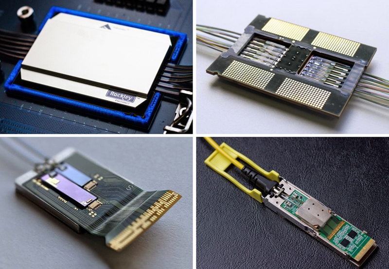
Products galore: Rockley Photonics’ optoASIC platform demonstrator (top left); underside depicting multiple 100G link optical fiber connectivity within package of silicon CMOS chip package (top right); Transmit-Receive Optical Sub-Assembly (TROSA) for data communication AOCs and transceivers depicting simplicity (bootom left); TROSA mounted in AOC, reference design, no package cover (bottom right).
| © 2026 SPIE Europe |
|