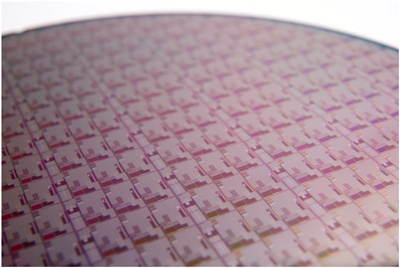
| A semiconductor wafer produced at IMEC, the world-leading research and development institute based in Leuven, Belgium, and recipient of the very first extreme ultraviolet (EUV) lithography tool, back in 2006. Thanks in part to key light-source developments at Cymer, EUV technology is edging towards commercial deployment for volume chip production over the next couple of years. Credit: IMEC. |
| © 2024 SPIE Europe |
|