 |

22 Jul 2010
Ten European consortia working on silicon photonics join forces to help transfer technology to electronics industry.
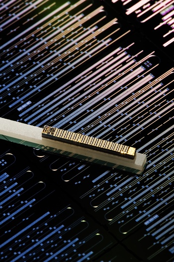
European experts working on various aspects and applications of silicon photonics are joining forces under a new umbrella group to help develop the technology commercially.
Ten different consortia, working on topics varying from integrated photonic routers to bacterial sensors, will co-operate as the European Silicon Photonics Cluster.
Although no new European funding has been received to set up the group, its aims include training young scientists and engineers involved in the emerging field, as well as organizing a workshop event on the topic in 2011.
Cluster spokesman Jean-Marc Fedeli told optics.org that there was no designated “leader” of the cluster. “This is a group that will meet regularly for better dissemination of silicon photonics activity,” he said. The full list of projects joining the cluster reads:
• Boom (silicon photonic integrated components)
• Historic (InP-on-silicon for optical routing and logic)
• Helios (Photonics/CMOS integration)
• Intopsens (Biophotonic sensors)
• PhotonFAB (Silicon photonics manufacturing platform)
• Platon (Plasmonic optical interconnects)
• SOFI (Si-organic active waveguides)
• UK Silicon Photonics
• Wadimos (WDM photonic layer on CMOS)
• Sabio (High-sensitivity biosensors)
Based at CEA-Léti in France, Fedeli is part of the Helios project, which is working to integrate photonics functionality on a CMOS silicon platform. Among the other members of this project are the Alcatel-Thales III-V Laboratory and the French optoelectronic component manufacturer 3S Photonics.
Fedeli highlights the semiconductor laser sources fabricated on silicon by Intel (in collaboration with the University of California, Santa Barbara) and CEA-Léti as two of the key recent developments in silicon photonics, as well as a silicon chip featuring a microlaser and microdetector developed under the Wadimos project in Europe.
But it isn’t just electronics and communications applications that the cluster will be focused on. Two biophotonics projects, Intopsens and Sabio, are set to develop optical sensors of pathogenic bacteria, and a highly integrated chip capable of multiple disease diagnoses.
Although Fedeli does not believe that the cluster will have any major impact on the European electronics industry in the short term, he says that the silicon photonics niche may provide an opportunity for smaller fabs.
“The thickness of the [material] layers are between those for microelectronics and MEMS manufacturing, so an adaptation of the process steps is required,” he explained. “More specifically, 193 nm lithography is a must for getting high-performance silicon photonics devices.”
Developing a manufacturing supply chain is already one of the key aims of the Helios project and this was also the case with earlier efforts such as Europic, so some initial building blocks are already in place, added Fedeli.
With the European microelectronics industry having lost significant ground to rivals in the US and Asia in recent years, the silicon photonics niche may represent an opportunity to strengthen the industry and gain a competitive advantage.
The cluster itself represents more than a €30 million ($36 million) investment via the European Union to re-invigorate European microelectronics.
“In establishing the cluster, the members agree that it is of strategic importance to maintain photonic chip design and chip integration functions within Europe, to improve Europe’s ability to compete globally,” it stated.
 |  |  |  |  |  |  |
| © 2026 SPIE Europe |
|


