|

09 Oct 2006
Start-up company MOXtronics has recently produced the first coloured ZnO-based LEDs. Although the efficiency of these LEDs is not high, improvements are rapid and the emitters have the potential to outperform their GaN rivals, say Henry White and Yungryel Ryu from MOXtronics.
The attractiveness of zinc oxide (ZnO) LEDs stems from the potential for phosphor-free spectral coverage from the deep ultraviolet (UV) to the red, coupled with a quantum efficiency that could approach 90% and a compatibility with high-yield low-cost volume production. One day these LEDs could even outperform their GaN-based cousins (which offer a narrower spectral range) thanks to three key characteristics – superior material quality, an effective dopant and the availability of better alloys.
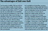
The superior material quality is seen in the low defect densities of ZnO layers. At MOXtronics, our development of a viable p-type dopant has provided hole-conducting layers for ZnO-based devices. And our growth of BeZnO layers has shown that it is possible to fabricate ZnO-based high-quality heterostructures ("The advantages of ZnO over GaN").
ZnO also promises very high quantum efficiencies, and UV detectors based on this material have produced external quantum efficiencies (EQE) of 90%, three times that of equivalent GaN-based detectors. The physical processes associated with detection suggest that similarly high efficiency values should be possible for the conversion of electrical carriers to photons. So it is plausible that ZnO LEDs will have an EQE upper limit that is three times higher than that of GaN-based devices.
Finding the right dopant
However, ZnO is yet to fulfill all of its promise because of the delay in developing p-doped material. Early progress throughout the community was hampered by focusing efforts on using nitrogen as a p-type dopant. Nitrogen was the first choice because it was an effective dopant in ZnSe, and also because it was deemed, erroneously, to be of a suitable size to sit on an oxygen lattice site. Although we also tried to obtain p-type doping using nitrogen, a switch to arsenic enabled us to report the first successful p-type doping of ZnO in 1997. By 2000 we could produce hole concentrations into the 1017 cm–3 range with this approach.
Later in 2000 we reported our hybrid beam deposition (HBD) process that offers a viable approach to growing doped and undoped ZnO films, alloys and devices. The HBD process is comparable to MBE. However, it uses a ZnO plasma source, which is produced by illuminating a polycrystalline ZnO target with either a pulsed laser or an electron beam, and a high-pressure oxygen plasma created by a radio-frequency oxygen generator. Additional sources for either doping or ZnO-based alloy growth can be added to the growth chamber by conventional evaporation or injection methods.
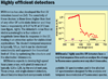
We used the HBD process to fabricate the first ZnO-based UV detectors ("Highly efficient detectors"), UV LEDs, FETs, and red, green, blue and white phosphor-coated LEDs. Our LEDs incorporate BeZnO, an alloy that allows bandgap engineering into the UV and the formation of multiple quantum wells and other heterostructures.
Why BeZnO beats MgZnO
BeZnO alloys of varying composition have significantly boosted the development of our deep UV high-power LEDs. These alloys do not phase-segregate, because BeO and ZnO have the same hexagonal crystal structures, and the extremely high-energy bandgap of BeO could potentially lead to devices emitting at just 117 nm. UV LEDs containing BeZnO alloys produce a narrow spectral profile, with very little emission in the visible, suggesting that the alloy is of high crystal quality.
Until we had produced BeZnO films, the primary choice for a compatible higher bandgap alloy was ZnMgO, a material developed by a group at Tohoku University, Toyo University, Tokyo Institute of Technology and Japan's Institute of Physical and Chemical Research. In 1997 this team reported that crystal phase separation occurs between MgO and ZnO when the atomic fraction of magnesium exceeds 0.33, which corresponds to a bandgap of 3.99 eV. The separation is driven by different crystalline structures; MgO is a cubic structure with a lattice spacing of 0.422 nm, while ZnO is a hexagonal wurtzite structure with a lattice spacing of 0.325 nm.
We recently produced and characterized the first UV LEDs made from ZnO and BeZnO. The device's emission can be tuned from the deep UV to around 380 nm, the wavelength associated with ZnO. Our devices have been built with several different active layer structures, including double heterostructures and single or multiple quantum wells, to try to improve efficiencies and optical output powers.
Our latest UV LEDs have a typical wall-plug efficiency of 0.1%, which would equate to an efficacy of 0.6 lm/W if the emission were in the visible spectrum. Although the efficiency is far lower than that of GaN LEDs, we are making rapid progress by addressing the various phenomena that degrade device performance. If progress continues at the same rate we will produce LEDs with a 1% wall-plug efficiency within one year, 1–5% within two years and about 10% or more within three years.
Our ZnO LED development programme has used various substrates manufactured by several vendors and has shown that the LED's performance is directly dependent on the substrate's material type and crystalline quality. Single-crystal ZnO produces the best devices. This material has been available for many years and interest is rapidly increasing for the growth of high-quality single-crystal ZnO with a diameter of 50 mm or more or ZnO-based LEDs and other devices.
What's needed
Major improvements in the efficiency and power output of ZnO UV and visible LEDs are still needed to enable these devices to compete in the market-place. Advances will depend on the availability of higher-quality single-crystal substrates and improved processes for producing reliable and highly ohmic electrical contacts to various different layers. Additional bandgap engineering development is needed for the UV C-band (100–280 nm) and visible region, along with optimization of the multiple quantum well and related structures in the device's active region.
Looking ahead
With the output power of our ZnO LEDs increasing rapidly, these devices appear to have a promising future. We expect them to first be deployed in white-light lamps and replace incandescent sources in applications such as liquid-crystal display backlights. The promise of emission from the UV through the visible will then allow ZnO LEDs to target applications where no other single semiconductor material can operate today. At this time, for example, red–green–blue sources that are fabricated on a single wafer will offer unique advantages for the development of bright, compact displays and projectors. Laser diodes built from ZnO-based materials could also be produced that emit in the visible and UV and offer compact alternatives for larger tube-type laser sources, ushering in a new era for colour printing.
• This article originally appeared in the August issue of Compound Semiconductor magazine.
 |  |  |  |  |  |  |
| © 2026 SPIE Europe |
|