|

18 Apr 2006
IBM announced last month that it had fabricated the smallest high-quality line patterns ever created by optical lithography. Jacqueline Hewett spoke to the researchers involved to find out how they did it and what the breakthrough means for the industry.
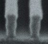
Up until last month, the consensus in the semiconductor industry was that optical lithography techniques would not extend beyond the 32 nm node. However, when IBM unveiled a pattern of 29.9 nm-wide distinct lines and spaces fabricated by a high-index immersion variant of 193 nm lithography, things changed.
The result suggests that optical techniques can be extended through the 45 and 32 nm technology nodes. What's more, IBM now believes that the high-index immersion approach buys the industry seven years of breathing space before it moves to alternatives such as extreme ultraviolet lithography.
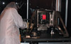
But just how did IBM fabricate the pattern? The answer is using an interference immersion lithography tool assembled in-house and called NEMO. The tool uses a combination of a narrow linewidth laser, precision optics, a high-index fluid and a clever mechanical design.
"We put together a team of individuals from various disciplines and started working on NEMO in December 2004," Bulent Kurdi, manager of nanoscale device integration at IBM's Almaden Research Center, told OLE. "Our first wafer came out of the system in June 2005. Then in November we incorporated a quartz crystal prism with a high refractive index and demonstrated the sub-30 nm pattern."
NEMO uses a simple optical set-up. A beam of linearly polarized 193 nm light is split into two coherent beams using a phase-grating. These beams are then directed along symmetrical paths towards the centre of the bottom surface of a prism. Both beams continue through a layer of transparent high-index fluid between the prism and the silicon wafer and overlap exactly at the resist-coated top surface of the wafer. This creates an interference pattern giving well-defined lines and spaces when the resist is developed.
It sounds easy, but each component of the system had to be carefully designed to meet strict tolerances. Starting with the laser, research staff member Don Bethune explains that the source needed to have a high degree of spectral purity. "We use a single-frequency Q-switched alexandrite laser that has a very narrow linewidth," he said. "It emits 100 ns pulses at 773.6 nm with a linewidth of less than 30 MHz."
Three nonlinear crystals convert the fundamental wavelength to a fourth harmonic at 193.4 nm. According to Bethune, the laser emits 2-3 W at 773.6 nm and produces 1-3 mW at 193.4 nm.
The first optical component that the incident light encounters in the NEMO tool is a phase-grating, which splits the light into two equal beams. Manufactured in-house, the grating is written into quartz and consists of a parallel array of trenches that are etched to a carefully controlled depth.
"Light going through the top of one of the trenches sees one path, whereas light passing through the bottom sees a slightly different path," explained Bethune. "We use the phase-grating to split the beam into diffractive orders. The zeroth order is eliminated. We use the two first-order beams, which the grating separates precisely and equally."
The two beams then follow symmetrical paths and are directed towards a prism. IBM has designed a set of prisms to create patterns with line widths starting at around 65 nm down to sub-30 nm. While the majority of prisms are made of fused silica, the one used in the sub-30 nm experiment was quartz crystal.
"Fused silica is disordered and slightly less dense so its refractive index is lower at 1.56," explained Bethune. "To get the very fine spacing you need a higher refractive index. Quartz crystal's physical density is higher and its refractive index rises to 1.67. The limit with a fused silica prism would be structures approximately 35 nm in size."
IBM's quartz crystal prism is trapezoidal and is approximately 4 cm wide, 1 cm thick and 3 cm high. According to Bethune, the angles in the prism have to be accurate to small fractions of a degree and the dimensions to a fraction of a millimetre.
The final essential ingredient is the immersion fluid. In standard immersion lithography, water is used between the prism and the wafer. But in order to demonstrate the sub-30 nm pattern and focus the light more tightly, IBM used a fluid with a refractive index of 1.64 from its collaborator JSR Micro.
Even after the optical design had been taken care of, Kurdi explains that there were several other factors to consider. "For example, you cannot allow any vibration," he said. "Any vibration on the order of 3 nm would introduce line edge defects that are 10% of the feature size you are trying to produce. Chemical contamination also spoils the photoresists so the tool resides in an environment with carbon filtration."
To overcome the vibration issue, IBM floats the wafer on a cushion of air when it is being translated between exposure sites. It then pulls a vacuum to lock the wafer in place during an exposure before re-pressurizing and moving the wafer frictionlessly to the next site.
According to Kurdi, it takes no more than one second to write a pattern over an area of a couple of millimetres. "A single wafer could have 100 exposure sites where something has been varied such as the exposure time or the height of the wafer below the prism," he said. "This is really where material studies come into play."
IBM is now using the NEMO tool to study both immersion fluids and photoresists. "We need to increase the refractive index of the fluid and the resist, and these are the two areas we are concentrating on right now," said Kurdi. IBM now hopes to increase the indices of refraction to 1.9, which would enable even smaller features to be imaged.
Kurdi admits that IBM has no immediate plans to commercialize the tool. "This is a very helpful tool when it comes to developing the materials needed for future immersion lithography," he said. "It is primarily intended to help understand photoresist behaviour - that's what it is really intended for inside IBM."
 |  |  |  |  |  |  |
| © 2026 SPIE Europe |
|