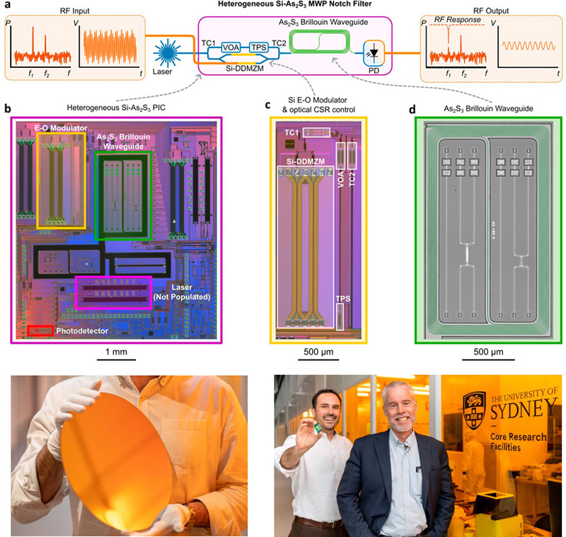
| Upper: Heterogeneous integration of As2S3 waveguides and silicon components for an on-chip microwave photonic filter system. Credit: Nature Communications (2023). Lower L: Silicon wafer used in chip manufacturing. Lower R: Dr Alvaro Casas Bedoya, holding the new chip, with Professor Ben Eggleton in the Sydney Nanoscience Hub. Photos: Stefanie Zingsheim. |
| © 2026 SPIE Europe |
|