 |
Date Announced: 04 Jul 2018
On the company’s main factory site to boost production capacity to meet increased demand for opto-semiconductors.
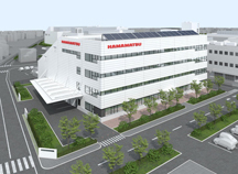
Hamamatsu City, Japan – Hamamatsu Photonics will construct a new factory Building No. 14 at the main factory site (Ichino-cho, Higashi-ku, Hamamatsu City, Japan) to meet growing sales demand for its opto-semiconductor module products.
The groundbreaking ceremony for the new factory building was held on June 26, 2018, and the new factory building will be completed in July 2019.
Hamamatsu Photonics has been supplying opto-semiconductors and module products that combine opto-semiconductors with electronic circuits, optical components and software for a wide variety of fields such as medical diagnosis and treatment, scientific measurements, and automobiles.
Recently, there has been vastly increasing demand for opto-semiconductor module products that can easily be assembled directly into equipment that customers manufacture.
This means that here at Hamamatsu Photonics we can expect a steady increase in sales of opto-semiconductor products including MPPC® (Multi-Pixel Photon Counter) modules for medical imaging devices, mini-spectrometers and optics modules for industrial equipment, and opto-semiconductor module products for automobiles.
Combine, consolidate and expand production
In the new factory building, along with consolidating our design & development departments for opto-semiconductor module products, which are currently dispersed in different locations at our main factory site, we will combine, consolidate and expand production space to enhance the development speed and production capacity of our opto-semiconductor module products.
We will also transfer our product warehouse and shipping functions to the new factory building so that all logistics functions including receipt of orders, procurement, warehouse operation and shipping will be clustered together within the main factory site.
This will help us improve business operational efficiency, information sharing and customer response speed. We also plan to boost production capacity of other opto-semiconductors such as image sensors, since free space available in existing factory buildings after clustering departments together in the new factory building will be utilized as space for production processes.
Based on our business continuity plan, this new factory building is designed with stronger disaster countermeasures that incorporate earthquake measures and flood measures such as waterproof doors, as well as environmental measures including installation of LED lighting, heat-insulating structures, and solar panels.
The building work was scheduled to start in June 2018 and will be completed in July 2019. The operation start date is expected to be October 2019.
The building structure is steel frame construction, 4 floors above ground, 1 floor underground. The interior building area will be 2,441 square meters, with a total floor area of 9,857 square meters, comprising an underground floor and three above floors
Opto-semiconductor modules
The new build will be used primarily for production of opto-semiconductor module products and design and evaluation of opto-semiconductor module products; it will also feature design rooms, conference rooms, rest area/lounge.
The total construction cost will likely be approximately 2.8 billion yen (around $25 million). The new building’s seating capacity will be approximately 240. Products to be made in th new facility will include opto-semiconductor module products. Overall its production capacity will be approximately 10 billion yen annually.
E-mail: info@hamamatsu.com
Web Site: www.hamamatsu.com
| © 2024 SPIE Europe |
|