22 Aug 2012
Technology that promises semiconductor lasers with on-chip polarization control developed by team at University of Glasgow.

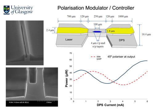
Design of Glasgow's semiconductor laser with monolithically integrated dynamic polarization control.
The team, led by Prof. David Hutchings, says that their monolithically integrated components can be controlled to produce any output polarization state from any input state whereby the resulting output polarization state can be switched electronically to any other state on the nanosecond timescale.
The research has previously demonstrated each of the constituent elements of the device and fully functional prototypes have recently been demonstrated. In principle this technology can be used at any wavelength where a semiconductor source exists, such as from the visible to the far infrared.
Prof. Hutchings told optics.org, “Among the application areas are telecommunications: the polarisation control device can be used to implement polarisation division multiplexing, increasing the capacity of an existing link. It can also be used to prepare an unknown polarization state to a specified one prior to a polarisation sensitive element such as a semiconductor optical amplifier.
”There are other applications in polarimetry: remote sensing; and in 3D laser projection displays: reducing the number of components required and providing the ability to employ laser arrays. We have had initial discussions with some companies in these areas but at this stage they have not yet been developed into a substantive collaborations.”
Current display systems based on passive 3D technology have an additional polarization modulation element in the optical path to produce two images required for the right and left eye. This integrated polarization control technology will offer improvements in 3D laser projector systems due to the removal of this component and the additional capability of being able to switch polarization of the laser source at high speed.
Communication applications
Polarisation control and manipulation are key functions in optical communications. This technology will allow the production of equipment with significant cost savings by lifting design constraints due to the necessity of polarisation independence. For polarisation multiplexed and coherent detection based long-haul systems a waveguide based polarisation control technology capable of integration with current designs will become a key enabling technology.
Hutchings added, “We have been working on waveguide polarisation mode converters for a few years, initially as an required element for an integrated optical isolator. However we realised that there were numerous applications in just being able to manipulate and control the polarization state.
”In 2009, we demonstrated and published that one of our polarization mode converters could be successfully integrated into a semiconductor laser giving a device, which emitted orthogonal polarisation states from either facet. We subsequently realised that by additionally integrating phase shift elements we could devise an integrated device which could dynamically control the polarization state. This was filed in a patent and we published the schematic in our 2011 IEEE Photonics Journal paper.
”Essentially we should be able to provide any polarisation state to the output by incorporating two 3dB polarization mode converters and two phase shift elements. We have recently carried out a proof-of-principle experimental demonstration, which has just been accepted for publication in Optics Express.
"On the same III-V chip we have successfully integrated a 1550nm laser, polarization mode converter and a phase shift element which operates by current injection and shown that the polarization state can be manipulated on a ~10s of nanosecond time-scale.
”Although the same principles are used with bulk optical components, we see the ability to integrate on a single chip as offering the advantages of: replacing manual assembly of components with lithography will improve yields, reduce costs, increase the number of devices fabricated, including the ability to fabricate an array of devices; the integrated device will be far smaller in volume with reduced power and drive voltage requirements and therefore can be accommodated within a vastly increased range of situations.”
About David Hutchings
Prof. David C. Hutchings [FInstP, SMIEEE] is a world-leading expert on nonlinear optics and optoelectronic integration in semiconductors and was appointed to a personal chair in Optical and Quantum Electronics at the University of Glasgow in 2004. His research interests and experience encompasses nonlinear optics, monolithic and heterogeneous optoelectronic integration, semiconductor theory and modelling, and computational electromagnetics.In 2010 he chaired the CLEO subcommittee 09 to which this proposed project corresponds. He served (2005–2010) as the Head of the Graduate School (Associate Dean) in the Faculty of Engineering, and provided leadership in Knowledge Exchange activities as the Eng.D. in System Level Integration Academic Programme Director.
About the Author
Matthew Peach is a contributing editor to optics.org
| © 2025 SPIE Europe |
|